In power supply design, engineers often face the problem of controlling the IC drive current shortage, or face the problem of excessive power consumption of the control IC due to gate drive loss. To alleviate this problem, engineers often use external drives. Semiconductor manufacturers (including TI) have off-the-shelf MOSFET integrated circuit driver solutions, but this is usually not the lowest cost solution. Discrete devices worth a few cents are usually chosen.
A simple buffer can drive more than 2Amps, and the FMMT618's higher current driver enhances drive capability.
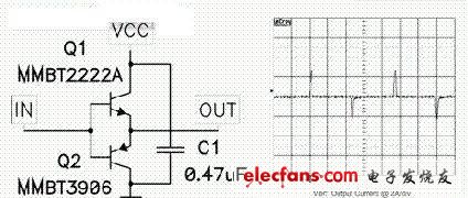
Figure 1
The schematic in Figure 1 shows an NPN/PNP transmit follower pair that can be used to buffer the output of the control IC. This may increase the drive capability of the controller and transfer drive losses to external components. Many people think that this special circuit cannot provide enough drive current.
As shown by the hf curve in Figure 2, manufacturers generally do not provide more than 0.5A for these low current devices. However, the circuit can provide current drive much higher than 0.5A, as shown by the waveform in Figure 1. For this waveform, the buffer is driven by a 50Ω source with a 0.01 uF capacitor in series with a 1Ω resistor. This trace shows the voltage across the 1Ω resistor, so the current on each post is 2A. This figure also shows that the MMBT2222A can supply approximately 3A and the MMBT3906 absorbs 2A.
In fact, the transistor will be paired with its components (MMBT3904 for 3906 and MMBT2907 for 2222). These two different pairs are for comparison only. These devices also have higher current and higher hfe, such as the FMMT618/718 pair, which has an hfe of 100 at 6A current (see Figure 2). Unlike integrated drivers, discrete devices are a lower cost solution with higher heat and current performance.
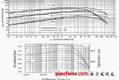
Figure 2: Higher current drivers such as the FMMT618 enhance drive capability -
Figure 3 shows a simple buffer variable case that allows you to cross the isolation boundary. A signal level transformer is driven by a symmetrical bipolar drive signal. The transformer secondary winding is used to generate buffer power and provide an input signal to the buffer. Diodes D1 and D2 adjust the voltage from the transformer, while transistors Q1 and Q2 are used to buffer the transformer output impedance to provide large current pulses to charge and discharge the FETs connected to the output. The circuit is extremely efficient and has a 50% duty cycle input (see the lower drive signal in Figure 3) because it will drive the FET gate negative and provide fast switching to minimize switching losses. This is ideal for phase-shifted full bridge converters.
If you plan to use an upper drive waveform of less than 50% (see Figure 3), then use a buffer transformer. This helps to avoid any low-to-zero transition of the EFT due to switching ringing, which can cause leakage inductance and secondary capacitance, which can cause ringing and produce a positive voltage outside the transformer.
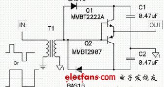
Figure 3: With a few components you can build a standalone drive
In short, discrete devices can help you save money. Discrete devices worth about $0.04 can reduce drive IC costs by a factor of 10. Discrete drives provide more than 2A of current and allow you to get power from the control IC. In addition, the device removes high switching currents in the control IC for improved regulation and noise performance.
Let's take a look at self-driven rectifiers and discuss when discrete drivers are needed to protect the synchronous rectifier gate from excessive voltage. Ideally, you can use a power transformer to drive the synchronous rectifier directly, but due to the wide input voltage variation, the transformer voltage can become so high that it can damage the synchronous rectifier.
Figure 4 shows a discrete device for controlling Q2 conduction in a synchronous reverse topology. This circuit allows you to control the turn-on gate current and protect the rectifier gate from high reverse voltages. This circuit can be driven with a negative voltage at the output of the transformer. The 12V input has a large negative voltage compared to the 5V output, causing Q1 to conduct and short the gate-to-source voltage on the power supply FET Q2, turning it off quickly. Since the base current flows through R2, there is a negative voltage across the accelerating capacitor C1. During this time, the primary side FET will conduct and store energy in the transformer magnetizing inductance. When the primary side FET is turned off, the transformer output voltage swings in the positive voltage range. The Q2 gate-source is rapidly forward biased through D1 and R1. When C1 is discharged, D2 protects the Q1 base-emitter connection. The circuit will remain in this state until the primary side FET is turned back on. Just like a synchronous buck converter, the output current actually discharges the output capacitor. Turning on the primary side FET attenuates the voltage on the secondary side of the transformer and removes the positive drive of Q2. This conversion results in a significant number of passes across the primary side FET and Q2 conduction. To minimize this number, Q1 will short the gate-source on the synchronous rectifier as soon as both the primary and secondary FETs are turned on.
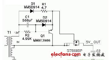
Figure 4: Q1 Quickly Close Synchronous Reverse -
Figure 5 shows a discrete driver for controlling the conduction of Q1 and Q4 in a synchronous forward converter. In this particular design, the input voltage is very broad. This means that the gates of the two FETs may exceed their rated voltage, so a clamp circuit is required. When the transformer output voltage is negative, the circuit turns on the Q4 diodes D2 and D4 to limit the positive drive voltage to around 4.5V. D1 and D3 turn off the FET, which is driven by the current in the transformer and inductor. Q1 and Q4 clamp the reverse gate voltage to ground. In this design, the FET has a fairly small gate inductance, so the conversion is very fast. Larger FETs may require a PNP transistor to decouple the gate winding of the transformer winding and increase the switching speed. Choosing the right package for the gate drive converters Q2 and Q3 is critical because these packages consume a large amount of power in the converter (this is because these packages act as linear regulators during the discharge of the FET gate capacitance). ). In addition, power consumption in higher output voltages R1 and R2 may also be high.
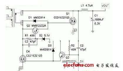
Figure 5: D2 and D4 limit the positive gate voltage in the synchronous forward driver
In summary, many power supplies with synchronous rectifiers can use the winding voltage of the transformer to drive the gate of the synchronous rectifier. A wide range of input or high output voltages requires an adjustment circuit to protect the gate. In the synchronous reverse structure shown in Figure 4, we show you how to control the reverse voltage on the synchronous rectifier gate while maintaining fast switching. Similar to the synchronous forward structure of Figure 2, we show you how to limit the positive drive voltage on the synchronous rectifier gate.
Our company specializes in the production and sales of all kinds of terminals, copper terminals, nose wire ears, cold pressed terminals, copper joints, but also according to customer requirements for customization and production, our raw materials are produced and sold by ourselves, we have their own raw materials processing plant, high purity T2 copper, quality and quantity, come to me to order it!
LYF Copper Lube Terminals,Ring insulated terminals
Taixing Longyi Terminals Co.,Ltd. , https://www.txlyterminals.com
