With the rapid development of network technology and communication technology, test instruments and test technologies have undergone revolutionary changes. "Network is instrument" accurately summarizes the network development trend between test instruments. The establishment of a networked test system not only enables resource sharing, but also facilitates the establishment of a system, and can also increase the complexity of the test system and broaden its application range. The author uses the CPLD chip to realize the IP core design of the GPIB controller to complete the property ownership of the chip NAT 9914, thereby greatly reducing the development cost.
1 GPIB controller scheme design
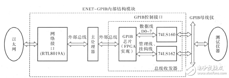
The General Purpose Interface Bus (GPIB) has unified standards for the interconnection of automated test instruments, greatly promoting the development of automated test technology. GPIB bus has parallel bus transmission speed, high effective data rate, strong driving capability, communication distance up to 20m, good anti-interference ability and versatility. Up to 15 devices can be connected on the bus and the transmission speed can reach 8Mbit / s. Therefore, there is a good application prospect [1], and its automatic test system is organized as shown in Figure 1.

  Figure 1 Block diagram of the automatic test system built into the GPIB controller
The GPIB controller IP core design adopts the modular idea. The main modules include state machine module, data path module and decoding circuit module. The design of the state machine module includes 8 small modules (such as source side hook and receiver hook). The VHDL language is used to program each small module. Finally, each submodule is called and the top level module design of the state machine is performed by the schematic diagram. And analyze and simulate on Synplify and Quartus II platforms. The same approach is adopted for the design of the data path. The sub-modules are designed first and then the overall design. Finally, the state machine top-level module, the data path top-level module and the multi-line message decoding circuit module are called to perform the top-level design of the GPIB controller IP core. After completing the entire IPCore design, the Core is downloaded to the selected DE2 dedicated development kit CPLD chip for communication setup verification through JTAG download. After successful, the hardware is built to obtain the materialized GPIB controller.
2 GPIB controller IP core design implementation
2. 1 interface control circuit works
The GPIB bus is a 24-pin parallel passive bus consisting of 8 ground lines and 16 signal lines. The 16 signal lines are 8 data lines (DIO1 to DIO8), 3 handshake lines (DAV, NRFD, NDAC) and 5 management lines (ATN, REN, IFC, EOI, SRQ). Data transmission adopts bit parallel, byte serial two-way asynchronous transmission. It should be noted that: GPIB uses negative logic, that is, low level (not greater than 0.8V) is logic 1, and high level (not less than 2.0V) is logic 0[2].
The basic principle of the GPIB bus is to use the controller as a server, to program and control each instrument through the GPIB bus. At the same time, each instrument also realizes the data transmission with the server by operating the GPIB control chip, and the signal output to the GPIB bus. It meets the IEEE488 standard for automatic control and testing purposes.
2. 2 module design
The design of the GPIB controller consists of three main modules: interface function module, multi-line message decoder and data path module.
2. 2. 1 Interface function module for communication with GPIB bus
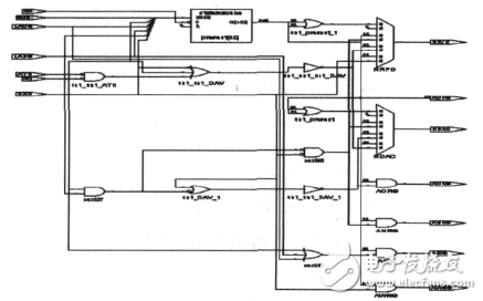
In the GPIB system, an interaction between the device and the GPIB bus is defined as an interface function, essentially a set of logic functions that implement the IEEE488 communication protocol. This function module is the focus of this design. It also has certain requirements in the selection of the interface function subset. It mainly implements the functions of each sub-interface, namely: source-side hook SH, speaker T, listener L, service request SRQ and remote control. This control RL and so on. Each interface module function is implemented by a synchronous MOORE state machine (only related to the current signal and independent of the input signal). On the basis of the function realization of each sub-interface module, the top-level state machine design is carried out, that is, each sub-module is called, and the interconnected design is implemented by schematic diagram, and the description of the state machine is completed by VHDL language. The function is shown in Figure 2. Among them, the input signals are: GPIB bus signal (ATN, DAV, IFC, REN, NDAC, NRFD, EOI, SRQ), multi-line messages (MTA, MLA, OTA, LLO, GTL, GET, DCL, SDC, UNL, SPD) , SPE), internal messages generated by the auxiliary registers and local messages (swrst, lon, rsv, ton). These input signals are generated by a decoding circuit that controls the state of the interface function.

Figure 2 GPIB bus communication function logic
The source side hook SH is taken as an example to illustrate the logic implementation. The logic diagram is shown in Figure 3.

Figure 3 Logic circuit implemented by SH function
The main code is:
IF RESET = '1'OR( NOT ATN AND NOT( LACS
OR LADS) ) = '1'THEN C_ST < = ST1; RFD <
= '1'; DAC < = '1';
AIDS < = ' 1'; ANRS < = ' 0'; ACRS < = ' 0';
AWNS < = '0'; ACDS < = '0';
ELSIF CLK'EVENT AND CLK = '0' THEN
CASE C_ST IS
WHEN ST1 = > IF ATN = '1'OR LACS = '1'OR
LADS = '1'THEN C_ST < = ST2; RFD < = '0';
DAC < = '0'; AIDS < = '0'; ANRS < = '1'; ...
ELSE C_ST < = ST1; RFD < = '1'; DAC < = '1';
AIDS < = '0'; ...WHEN .... ELSIF DAV = '1' THEN C_ST < = ST4;
RFD < = '0'; ...
ELSE C_ST < = ST2; RFD < = '0'; DAC < = '0'; ...
...different kinds of state definitions...
2. 2. 2 data path module design
The module realizes the data from the microprocessor end to the GPIB interface function end, and reads and writes the internal register of the controller.
2. 2. 3 multi-line message decoder circuit
The purpose of the decoding circuit is to generate a logic function signal, decode the remote message and the local message sent by the controller, and realize the control of each interface function.
2. 3 programming
The programming mainly completes the interface initialization, the main control PC sends a message to the instrument, and receives the message and analyzes and processes the data. All kinds of actions on the bus are written or read to the internal registers of NAT9914 through the PC, so that the interface realizes corresponding function changes.
2. 4 Experimental results
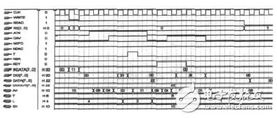
Through the construction of the overall system, the data transmission between the instrument and the bus is completed. The experimental results are analyzed by taking the AH and L functions in conjunction with receiving data from the GPIB bus. The AH and L function receives data. The experimental result waveform is shown in Figure 4.

Figure 4 Receiver receives data waveform
As can be seen from Figure 4, the signal WRITE and the address RS [2. . 0] = 010 (the address of the ADR in the register), the instrument passes INDATA[7. . 0] The data port writes the address 11H of the instrument on the GPIB bus to the address register ADR. On the 4th clock falling edge, the device receives the ATN signal, indicating that the AH function enters the ANRS state from the AIDS state; the 5th clock falling edge still has the ATN signal, indicating that the AH function enters the ACRS state from the ANRS state, and sends an RFD signal, telling The controller is ready to receive GPIB interface commands; on the falling edge of 6 clocks, the DAV signal transmitted by the bus is detected, indicating that the AH function enters the ACDS state from the ACRS state. Subsequently, the system controller sends the address command 31H through the DIO line, and outputs the MLA signal through the multi-line message decoder. On the falling edge of the 7th clock, the L function enters the LADS state from LIDS under the action of MLA&ACDS, indicating that the instrument has been assigned to Listener, after receiving the interface message, a T signal will be generated; on the falling edge of the 8th clock, the GPIB controller detects the T signal, indicating that the AH function enters the AWNS state and issues a DAC signal, telling the controller that the interface command is accepted. At the 9th clock falling edge, the system controller cancels the DAV signal and the ATN signal, indicating that the AH function enters the ANRS state, and the process of a three-wire hook has been completed. When the ATN is 0, the L function enters the LACS state, and the instrument officially enters the listener state. The other transmission process is similar to the process of receiving data by the listener, and will not be described here.
3 Conclusion
The experiment proves that the automatic test system consisting of GPIB controller has the characteristics of automatic data acquisition, fast speed and high efficiency. Its core components are portable with IP core design, which can be short in development cycle and low in cost, which changes the manual operation of traditional instruments. And the shortcomings of single use, and the automatic test system combining computer and instrumentation provides a powerful medium for intelligent and standardized development.
Adjustable Aluminum Laptop Stand, Nulaxy Adjustable Aluminum Laptop Stand, Amazon Aluminum Laptop Stand
Shenzhen ChengRong Technology Co.,Ltd. , https://www.dglaptopstandsupplier.com
