
Researchers from Dalian University in China have developed a new process that can build fully transparent flexible circuits for any pattern on demand. The circuit pattern is completed on a transparent flexible substrate by a mature microfluidic technology.
The conductor is generated by spin-coating silver nanowires along the pattern. Research progress will have a greater impact on future electronic products. Future electronic devices are generally assumed to be transparent and flexible, such as transparent flexible computers, touch screens, cell phones, and wearable medical devices. Transparent flexible circuits are an important part of this type of equipment. However, due to two major challenges in the field of transparent flexible circuits, completely transparent flexible circuits are difficult to achieve. One of the challenges is that both the conductor and the substrate are transparent, and the second challenge is ultra-precise pattern control. The publication “Highly Transparent Flexible Circuits for Patterning Silver Nanowires into Microfluidic Channels†published in Chemical Communications for the first time demonstrates that a completely transparent flexible circuit can be manufactured with a friendly protocol. It also exhibits excellent transparency, conductivity, stretchability, twistability, ultra-precise pattern control, and features that can be mass-produced. The study was also selected as the back cover of the journal.
Microfluidic technology is a technology that handles very small volumes (eg, nanoliters) of fluids. Researchers formed transparent flexible circuits by coating silver nanowires into microfluidic channels. The fluid is wrapped in so-called microfluidic channels (a soft and optically transparent material). Silver particles and silver nanowires are good materials for constructing transparent and flexible electrodes. However, prior art generated circuits either lack pattern control (via nanoparticles) or have problems with optical opacity (via nanowires).
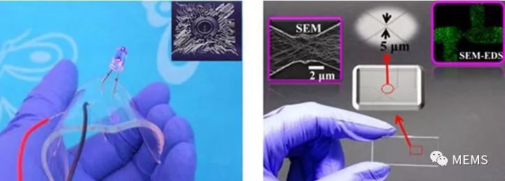
The left image shows a light-emitting LED on a transparent flexible circuit with a complex pattern (upper right illustration), and the right image shows the use of a scanning electron microscope (SEM, top left illustration) and scanning electron microscopy (SEM-EDS, top right illustration). An enlarged, thin circuit (5 micron wide) indicates that the conductors are evenly and continuously distributed throughout the circuit, including the narrowest part (5 micron) Professor of Analytical Chemistry at Dalian University, co-author of the research paper, Dr. Jing Sun, said, "We The research has both the advantages of microfluidic technology and silver nanowires, silver nanowires are dissolved in non-toxic solvents such as water and ethanol, and silver nanowire solutions are then filled into the microfluidic channels by conventional coating methods.
Since microfluidic channels can be precisely created at the nanometer level, the resulting circuit can become more complex and the design of the pattern can become more accurate. “Wenhui Zhou, a postgraduate of Dalian University and the second author of the paper, pointed out that the circuit made of silver nanowires has high conductivity and transparency. The circuit can also withstand repeated bending, twisting, and stretching. “Furthermore, since the conductive part of the circuit is located in the channel, the circuit is very durable compared to laying silver nanowires on the surface only,†added Dr. Ming-Fei Lang, professor of basic medicine at Dalian University. "Besides, these circuits are easy to produce, scalable, and reproducible, so these features are suitable for mass production. The researchers have demonstrated the circuit as a simple application of glucose detection biosensors. A provisional patent for this technology has already been submitted, and Sun said, “With optical, mechanical, and electrical properties, our technology can produce transparent flexible circuits with controllable patterns, scalable dimensions, and reproducible quality characteristics.
We are looking forward to our process approach to contribute to the potential application of wearable medical devices and transparent electronic devices. "This study was funded by the National Natural Science Foundation of China (Project Grant No. 21505013) and the Natural Science Foundation of Liaoning Province (Project Grant No. 2015020660).
The through-wall terminals can be installed side by side on panels with thicknesses ranging from 1mm to 10mm, and can automatically compensate and adjust the thickness of the panel to form a terminal block with any number of poles. In addition, isolation plates can be used to increase air gaps and creepage distances.
Through-Wall Terminal,Through Wall Terminal Block,Through-Wall Terminal Extender,Through-The-Wall Terminal Block
Sichuan Xinlian electronic science and technology Company , https://www.sztmlchs.com