The difference between the hardware logic and the software program in the FPGA, I believe we will have a deep understanding when doing division operations. If one of the operands is a constant, it can be replaced by a simple shift and sum operation, but using hardware logic to complete the division between two variables will consume more resources, the circuit structure is complex, and usually cannot be completed in one clock cycle. . Therefore, FPGA implementation of division operation is not a "/" sign can be solved.

Fortunately, these basic operations all use free IP cores. The VIVADO 2016.4 development environment provided by the author uses the AXI bus interface for the divider gen IP cores. The naTIve interface is no longer supported. Therefore, the focus of the division operation has changed from the design of the algorithm circuit to the call of the AXI bus IP core and the representation of the signed number in the HDL, which greatly reduces the development difficulty. The following two aspects are discussed.
The default data type in Verilog HDL is an unsigned number. Therefore, if a mathematical operation is required, a “signed†statement must be used. For example: reg signed [8-1:0] signal_a; wire signed [32-1:0] signal_b; At one point, the FPGA treats all signed numbers as two's complement and the result of the operation is also the complement. Let's look at the divider IP core configuration interface.


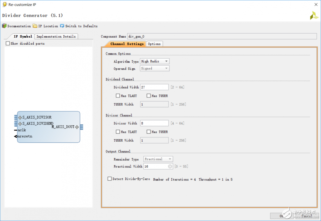
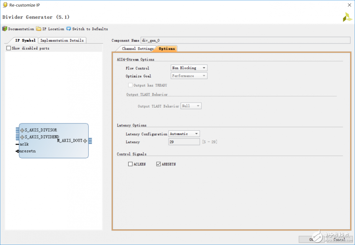
A total of two pages are very simple. There are three places that need to be focused on: 1 Algorithm type 2 Bit width of dividend and divisor 3 Page 2 Flow control mode. I now explain one by one:
In terms of algorithmic structure, the official document pg151 LogiCORE IP Product Guide describes in detail: The LUTMult structure operand is better not to be higher than 12bit, and make full use of DSP slice and BRAM to reduce the consumption of FPGA logic resources. Radix-2 operands should not exceed 16 bits, and the use of resources, in contrast to LUTMulTI, uses a large number of registers and LUTs to save DSP slice and BRAM resources for use elsewhere. The last High Radix architecture supports large bit-wide operands in excess of 16 bits, using dedicated hardware resources such as DSP slices. Choose according to your needs.
The bit-width problem has nothing to say, and it needs to pay special attention to the reserved bit width that satisfies the calculation range, that is, the "complement sign bit extension" before the operation. As for the flow control mode and the interface and AXI bus.

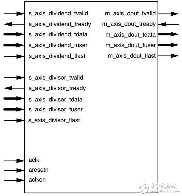
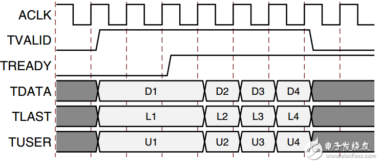
The interfaces are clearly divided, the dividend divisor and quotient channels, and the necessary clock and reset logic interfaces. Each AXI bus channel always includes tdata tuser tlast and handshake signal tvalid tready, where tuser is additional information and tlast represents the last data in streaming mode, which is equivalent to the end of packet in the data packet. The data transfer is valid and updated only when tvalid and tready are pulled high at the same time.

The Non Blocking Mode is more commonly used in the division operation. In a word, the IP core interface does not have a FIFO buffer, and the output channel data must be processed in real time by a downstream module. The above figure will understand:

This mode is actually a simplification of the AXI bus. In many cases, the powerful flow control function of the AXI bus is not completely required, especially when the AXI bus module is an FPGA logic circuit that can perform real-time processing. Another feature of the AXI bus is data packing. It is necessary to fill in the upper bits of data that are not 8 bits wide to ensure that the minimum unit of data is 1 byte. The specific filling method is different. It is easy to think that such a data packing function is very friendly to the interaction of the PL and PS sections in the SOC.
In general, it is not difficult to do basic mathematical operations in FPGAs. Even complex operations such as exponential logarithm are supported by floating-point IP Core.
Android is an open source mobile operating system based on Linux platform released by Google at the end of 2007, and then improved for use in netbooks and MIDs. The platform consists of operating system, user interface and application software, and is claimed to be the first truly open and complete mobile software for mobile terminals.
To put it simply, the Android system is actually a very open system. It can not only realize the functions of the most commonly used notebook computers, but also realize various directional operations like mobile phones. Moreover, it is specially designed for mobile phones. The operating system developed for equipment has advantages in system resource consumption and human-computer interaction design. It is an operating system that combines traditional and advanced advantages.
New Android Tablet,Android Tablet,New Android Tablet
Jingjiang Gisen Technology Co.,Ltd , https://www.gisentech.com
