
CLB is the main logical resource for implementing sequential and combined circuits.
Virtex-6 contains two SLICEs in each CLB module. Each CLB is connected to an external general-purpose logic array through a switch matrix, as shown in Figure 5-2 and Figure 5-3. There is no direct connection between the two SLICEs in the CLB.
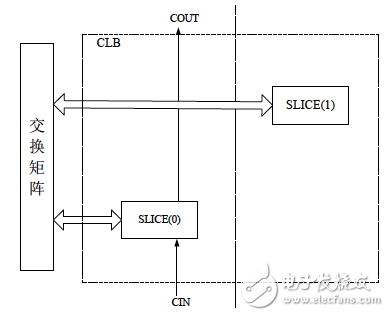
Figure 5-2 SLICE arrangement in CLB
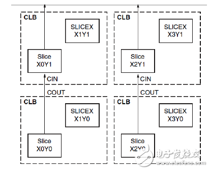
Figure 5-3 Position of the CLB
In Virtex-6, SLICE is divided into SLICEX, SLICEL and SLICEM. SLICEX has no storage function and no carry chain; SLICEL does not have storage function, but contains carry chain; SLICEM has storage/shift register function, also includes Carry chain.
Each SLICE contains 4 LUTs and 8 storage units. These basic units provide logic, arithmetic, and ROM functions. In addition to these basic functions, there are some SLICEs with distributed RAM and shift register functions. These SLICEs are also known as SLICEM.
The CLB can implement the functions shown in Table 5-1.
The SLICE structure diagram is shown in Figure 5-4(a) and Figure 5-4(b). Each SLICE contains a logic function generator (ie LUT), a storage element, a multi-function multiplexer (MUXF), and a carry. Resources such as logic and algorithm units (MULT_AND).
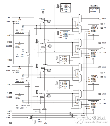
(a) SLICEM
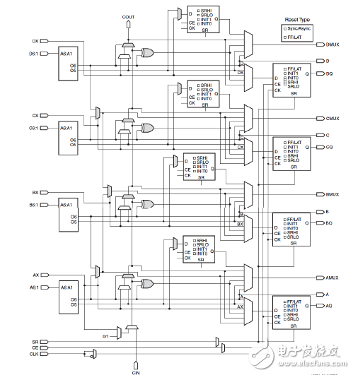
(b) SLICEL
First, the lookup table (LUT)The function generator of the Virtex-6 FPGA is implemented by a 6-input lookup table. Each LUT has 6 independent inputs (A1-A6) and 2 independent outputs (O5 and O6) that can implement any 6-input Boolean function. At the same time, each LUT can also implement 2 arbitrary 5-input Boolean functions under the same input conditions. If it is a 6 input function, only O6 is output.
O5 and O6 correspond to the outputs of the two 5-input function generators, respectively, in which case A6 is set high by software. The delay of the LUT is independent of the function implemented.
The LUT can implement functions such as combinatorial logic, ROM, distributed RAM, and shift registers.
(1) Combinational logic: All LUTs can implement any of the 6 input Boolean functions.
(2) ROM: All LUTs can implement a 64&TImes; 1-bit ROM. There are three configuration methods, namely ROM64 & TImes; 1, ROM128 & TImes; 1 and ROM256 & TImes; The ROMs in SLICEM and SLICEL can be cascaded into wider or deeper ROMs. See Table 5-2 for the configuration table.
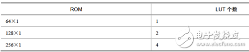
Table 5-2 ROM configuration
(3) Distributed RAM memory (used only in SLICEM): The LUT in SLICEM can be configured as a synchronous RAM called distributed RAM. Multiple LUTs in SLICEM can be flexibly combined to store more data. The RAM component can be configured in the following form in SLICEM. The configuration of the RAM is shown in Table 5-3.
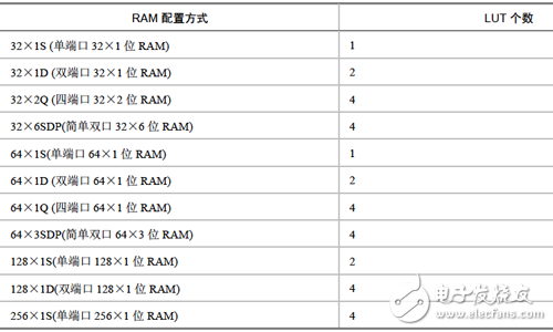
Table 5-3 Configuration Table of Distributed RAM
The distributed RAM primitives are shown in Table 5-4.
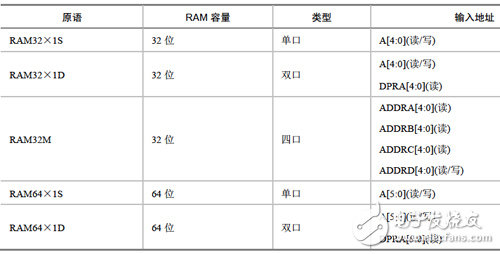
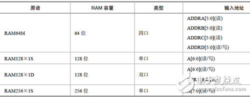
Table 5-4 Primitives of distributed RAM for single, dual, and quad
(4) Shift register (can only be used in SLICEM): SLICEM's LUT can also be configured as a 32-bit shift register, eliminating the need to use the trigger provided in SLICE. LUTs used in this way can delay serial data by any length between 1 and 32 clock cycles. The shift register shift input SHIFTIN and shift output SHITOUT are used to cascade the LUT into a larger shift register. The four LUTs in a CLB can be cascaded to generate a delay of 128 clock cycles. The CLBs can also be connected to form a shift register for balancing the timing of the data pipeline. The shift register primitives are shown in Figure 5-5.
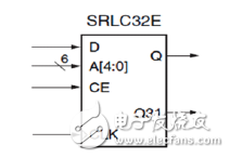
Figure 5-5 Primer of the shift register
Second, the storage componentEach of the Virtex-6 SLICE has a memory component that implements a memory function that can be configured as an edge-triggered D-type flip-flop or a level-sensitive latch, as shown in Figure 5-6.
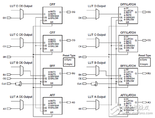
Figure 5-6 Register/Latch Configuration in SLICE
Third, multiplexer (MUX)In a SLICE, in addition to the LUT, there are three multiplexers (F7AMUX, F7BMUX and F8MUX), and the user can combine the four function generators to form a 7-input or 8-input function. Functions with more than 8 inputs can be implemented with multiple SLICEs.
Multiplexers F7AMUX, F7BMUX, and F8MUX typically implement a variety of multiplexers along with function generators or on-chip logic. The following multiplexers can be implemented.
1 LUT implements 4:1 multiplexer
2 LUTs implement 8:1 multiplexer
4 LUTs implement a 16:1 multiplexer
Fourth, fast first bit logic (Carry Logic)Virtex-6 has two independent carry chains for each CLB, which is used to implement fast arithmetic addition and subtraction. It solves the delay problem of multi-bit wide addition and multiplication from the lowest bit to the highest bit. The first carry bit logic has a dedicated carry path and a carry multiplexer (MUXCY) that can be used to cascade function generators (LUTs) to implement wider and more complex logic functions and improve the processing speed of the CLB module. The carry chain in Virtex6 is the upper travel bit chain, and each SLICE has a height of 4 bits. Considering the upstream structure of the carry chain, in the design, pay special attention to the length of the carry chain, because if the length of the carry chain exceeds one column, the carry chain will cause the delay to become much longer, affecting the timing.
Five, arithmetic logic (MULT_AND)The arithmetic logic consists of an exclusive OR gate (XOR) and a dedicated AND gate (MULT_AND). An XOR gate allows a SLICE to implement a 2-bit full-add operation, and a dedicated AND gate improves the efficiency of the multiplier.
Solar Panel Robot,Solar Cleaning Robot,Robot For Solar Panel Cleaning,Self Control Cleaning Robot
GuangZhou HanFong New Energy Technology Co. , Ltd. , https://www.gzinverter.com