1.1 CC2531
The CC2531 is a USB-enabled system-on-a-chip (SoC) solution for IEEE 802.15.4, ZigBee, and RF4CE applications. It is capable of building powerful network nodes at very low total material costs. CC2531 integrates 2.4 G. Hz RF transceiver, enhanced industry standard 8051 MCU, in-system programmable 256 KB Flash, 8 KB RAM and many other powerful features; transmit power of 4.5 dBm (adjustable), receiver sensitivity is -97 dBm.
1.2 CC2591
The CC2591 is a highly integrated RF front-end chip from TI that operates at 2.4 GHz for low-power and low-voltage wireless applications. The CC2591's internal integrated power amplifier (PA) has a gain of 22 dB, a maximum transmit power of +22 dBm (input +5 dBm), an output 1 dB compression point of +19 dBm, and the receiving part's internally integrated LNA sub-high and low receive gains are 11 dBm, 1 dBm, noise figure 4.8 dB, and improved receive sensitivity by 6 dB.
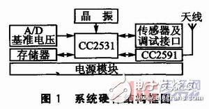
2 overall designAccording to the design requirements, the system hardware block diagram is shown in Figure 1. The core chip CC2531 combines its peripheral circuits (such as crystal oscillator, A/D reference voltage, memory, sensor and debug interface), plus the necessary power module and RF front-end chip CC2591, which constitutes the hardware system of this solution. When applied to different fields, the corresponding sensor, power supply, A/D reference voltage, memory, etc. can be adjusted accordingly. The hardware design of the CC2531 and CC2591 parts is relatively fixed.

3.1 Transmit power budget
According to the data sheets of CC2531 and CC2591, the transmit power of the CC2531 RF port is up to +4.5 dBm. Modify the TXPOWER register value to adjust its transmit power, ranging from -22 to +4.5 dBm. When CC2591 is connected, the PA gain in the CC2591 transmit mode is up to 22 dB, and the corresponding transmit power range is +22 to 10 dBm (the maximum value is determined by the PA itself, and the minimum value can be smaller). Considering the PA's 1 dBm compression point (19 dBm) and system power consumption, the TX-POWER=0xD5 is set, that is, the output power of CC2531 is 1 dBm, and the transmission power of CC2591 is 19 dBm. Power output reference setting (for reference only, there may be changes in practice).
3.2 Receive sensitivity estimation
When the CC2591 is in the receive high gain mode, HGM=1, its external antenna together with the internal T/R selector to the internal LNA has a noise figure NF of 4.8 dB, and the signal-to-noise ratio SNR of the internally resolvable signal of the CC2531 is 3 dB (guaranteed bit error rate is at a certain level), single channel transmit and receive bandwidth BW can be set to 1 MHz or 5 MHz. According to the formula, when the normal room temperature T0=290 K, the noise power of the 1 Hz bandwidth is N0=-174 dBm, and the receiving sensitivity is S=-174 dBm+NF+SNR+10log(BW). Substituting parameters can be obtained: when the receiving bandwidth is 5 MHz, the receiving sensitivity is S=-99.2 dBm.
3.3 Communication distance estimation
In the real environment, communication between any two points, the loss caused by the environment to the transmission wave is generally not quantitatively estimated, and varies greatly depending on the environment. Under the condition that electromagnetic waves are transmitted under ideal conditions without considering external influences and transmission losses, the calculation formula of wireless communication transmission distance is as follows:
Loss=32.44+20lgd+201gFreq
The antenna gain is not considered at this time (depending on the actual purchase of the antenna parameters). The link loss budget Loss is 118.2 dBm (excluding non-ideal loss), and the frequency Freq is calculated by the CC2531's RF center frequency of 2450 MHz, and the wireless communication transmission distance d=7.93 km is obtained. This distance is not reached in practical applications. This value is for reference only.
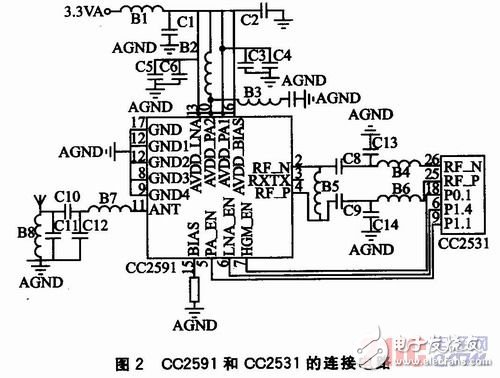
4 wireless communication module principleThe main peripheral circuits of CC2531 mentioned in the overall block diagram are not introduced here. The connection circuit of CC2531 and CC2591 is shown in Figure 2. These include the matching link of the RF differential signal line between the chips, the matching circuit of the RF signal to the antenna, the CC2591 control signal line, and the decoupling filtering part of the power supply.
Among them, the decoupling filtering part of the power supply line, B1 is a magnetic bead, and the frequency range of effective filtering should be paid attention to when selecting. At the same time, other components should also be selected for high frequency capacitors and inductors. The RF signal is connected to the matching circuit part of the antenna. The connection port of the antenna uses the SMA interface (female). It can be used to make the spectrum analyzer and the vector network analyzer more convenient for circuit measurement. It can also be connected with the antenna corresponding to the SMA connector. . For the three enable controls of CC2591, the assignment is as follows: P0.1→HGM_EN, P1.1→PA_EN, P1.4→LNA_EN. Among them, P0.1 that controls HGM_EN can be replaced by any GPIO, and the other two cannot be changed. They are mapped to the system protocol stack internal interfaces and registers, respectively.
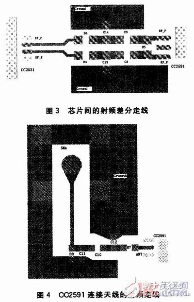
5 PCB circuit implementationCompared with the design of the schematic, more practical and practical problems will be encountered in the actual design and production of PCB boards. According to the schematic diagram given in Fig. 2, the wiring of the RF signal line portion is designed. Figure 3 shows the RF differential traces between the chips. Figure 4 shows the RF traces for the CC2591 connected antenna. Figures 3 and 4 show the layout of the RF traces, using the most common island wiring in RF. Because its operating frequency is 2.4GHz, and the maximum power reaches 20dBm level, there is not much reflection in the schematic diagram, but in the PCB, due to the unreasonable wiring, the large reflection and energy accumulation in some places may be caused. Lead to design and production failures. Therefore, all RF signal lines are designed to be as straight as possible.


The SMA connector is used for the antenna connection. In Figure 4, the part connecting the component B8 and the SMA connector is a 50 Ω microstrip line, and impedance control is required in actual production. Finally, the design of the surface copper floor is to ensure a good grounding of the RF signal. During the actual production of the PCB design, since the parameters such as dielectric constant and medium height cannot be ideally set according to the expected setting, there will inevitably be deviations. Therefore, it is necessary to pay attention to the parameter changes and adjust them in time. Set single channel transmission, CC2531 internal TXPOWER=0xD5 (typical transmission power +1 dBm), and measure the center frequency at 2.401 GHz, the power is +19.21 dBm. Although affected by other factors, this result is larger than the predetermined output power, but acceptable. The results show that the transmission of the RF link part of the system is ideal, and the reflection and loss control in the actual circuit is within the engineering acceptable range. The corresponding receive link can also predict that its reflection and loss are acceptable.
ConclusionAccording to the actual requirements, a wireless sensor network node that increases the transmission power to increase the transmission distance is designed and produced. From the measured data, it can be seen that the addition of the power distribution unit does greatly increase the transmission power of the node. Due to the limitations of equipment and measurement conditions, the measurement of some other parameters has not been carried out. This is a place to be perfected in the future. Improvement of the circuit is also one of the focuses of future work.
TPU Cutting Machine Accessories
Cutting Head Parts suitable for Screen Protector Cutting Machine.
The Cutting Blade can be used to cut Hydrogel Screen Protector, Back Film, Watch Screen Protector, etc. The quality of the Accessories For Cutter is higher than that of stainless steel, sharp and durable, and can be cut for a long time. In addition, the blade is protected by a plastic cover to avoid scratching your fingers.
Cutting Blade Parts For Screen Protector Cutter,Cutting Tip For Screen Protector Cutting Machine,Mobile Phone Screen Protection Cardboard Scraper Tool,Scraper For Film Cutting Machine
Shenzhen TUOLI Electronic Technology Co., Ltd. , https://www.hydrogelprotectors.com
