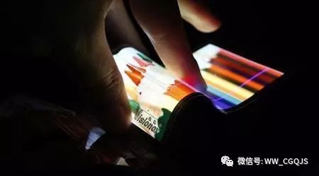
The flexible display is a very promising display technology. Through the efforts of many researchers and engineers, flexible display technology has developed rapidly. In the near future, the development of flexible display technology will make the display of information more flexible and diverse. At present, the main technologies for implementing flexible display include: liquid crystal display (LCD), organic light emitting devices (OLED), and electrophoretic display (EPD).
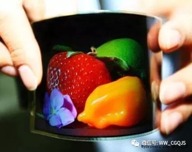
The development of flexible LCDs has been at an early stage. One problem that has always been faced is that the cell gap has a great influence on the LCD display. As the flexible substrate is bent, the cell gap changes to affect the display effect of the LCD. Until the discovery of new liquid crystal materials (such as cholesteric liquid crystals), flexible LCDs have developed rapidly.
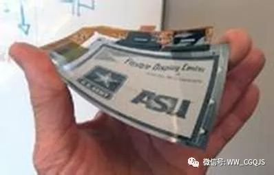
Unlike flexible LCDs, flexible EPD displays utilize a thin layer of illuminated electronic ink that has millions of tiny microcapsules in the electronic ink liquid. Inside each capsule is a mixture of dye and pigment chips, which can be charged by a charge. The flexible EPD display is mainly used in the field of electronic reading. E-ink's electronic inks are favored by major panel manufacturers, and many panel manufacturers have introduced EPD display anodes.
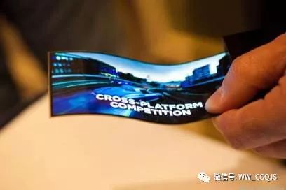
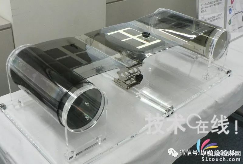
The application of OLED in flexible display has unique advantages. The properties of materials used in ultra-thin, all-solid and OLEDs are well suited for flexible displays. At the same time, the preparation process of the OLED is mainly evaporation, spin coating, and printing, and these processes can all realize deposition of a thin film on a flexible substrate. In particular, the development of solution methods for the preparation of OLEDs enables them to be well combined with a roll-to-roll process to produce low cost large size OLED display devices.
Development of flexible display technology
In 1974, Xerpac Palo Alto Research Center Gyricon e-paper
2003-2005 Xerox is ready to commercialize Gyricon
2005-2008 HP flexible display
In 2007, Sony flexible OLED was born
In 2008, the Nokia morph screen appeared Nokia 888
In 2011, the first user-grade curved screen phone was unveiled. The phone name was “bendyâ€.
Phone"
In 2012, NanoLumens introduced the first NanoFlex 112-inch large curved screen
In 2013, Samsung unveiled YOUM at CES (ConsumerElectronics Show)
In 2013, LG released the first truly mass-produced curved flexible screen phone LG G-Flex
In 2014, LG exhibited a 77-inch curved OLED UHD TV at CES
From the perspective of the current three flexible display technologies, the main problems faced by flexible LCDs are reflected in the backlight design of flexible substrates and the uniformity of display viewing angle display. The colorized display of the flexible EPD display is one of the concerns, and the corresponding speed of the EPD display is slow, so the application in animation and video has certain limitations. The key issue facing flexible OLEDs is that OLED devices themselves are sensitive to water and oxygen, and effective packaging is a hot spot for research and development. Meanwhile, for flexible display, a common problem is the preparation of a TFT device on a flexible substrate.
Flexible display substrate material
In flexible display devices, flexible substrates are the basis for developing flexible displays. According to the current research progress of flexible display substrates at home and abroad, flexible display substrates are mainly divided into five categories: plastics, metal foils, ultra-thin glass, and paper substrates and biocomposite film substrates which have recently attracted wide attention of researchers. These substrates provide device performance close to that of conventional glass substrates and are important for developing flexible displays for most applications using very low cost flexible substrates.
Plastic substrate
Plastics are considered to have broad prospects as flexible substrates because plastic substrates have the advantages of transparency, flexibility, light weight, durability, and low cost. Plastic substrates incorporating modern precision technology contribute to the growth and printing of organic light-emitting polymers and active-matrix thin film transistor arrays, providing cost-effective, roll-to-roll high-volume processing possibilities for large-scale integration of flexible electronic devices.
Plastic substrates are generally divided into three categories:
1. Semi-crystalline thermoplastic polymers such as polyester (PET), polyethylene terephthalate (PEN), polyetheretherketone (PEEK). PET and PEN as flexible substrates exhibit some important properties, including inherently good transparency, simple processing, good mechanical properties, high barrier oxygen and water vapor permeability, but they are not resistant to high temperatures, low temperature deposition of ITO When the device performance is degraded. When the temperature is raised, such a polymer substrate shrinks, and the ITO film is easily peeled off from the substrate; the surface roughness thereof is also relatively large, and the film deposited on the polymer substrate is liable to cause defects.
2. A non-crystalline polymer such as polyethersulfone (PES). PES is a non-crystalline thermoplastic that can be melt extruded or solvent injected. It has good transparency and a high working ceiling temperature, but it is expensive and has poor solvent resistance.
3. Non-crystalline high glass transition temperature (Tg) polymers, such as PAR, PCO, PNB and PI, PI has good thermal stability, good mechanical properties and chemical properties, but low transparency and relatively expensive. Fabric materials can also be used as flexible substrates.
The performance of the currently used polymer flexible substrates is shown in the table.

Stainless steel substrate
Stainless steel substrates are generally used in flexible luminescent displays where transmission requirements are not very high. If applied to large displays, it is a very expensive material, and it is expected to be used in small flexible displays. The high temperature resistance of stainless steel substrates (at least above 1000 ° C) is much higher than that of plastics and glass. The use of metal foil substrates in the process of making flexible displays does not present heat resistance problems. Therefore, stainless steel substrates are also a common choice, even including chemically inert titanium foils. The comparison of the performance of the stainless steel substrate with other substrates is shown in the table.

As can be seen from the table, the stainless steel substrate has good electrical conductivity, excellent water vapor and oxygen barrier properties with respect to the plastic substrate, a higher thermal expansion coefficient of lower modulus of elasticity, and can be mass-produced by R2R. However, a rough-surfaced foil cannot be used directly as a flexible substrate, otherwise it will affect the performance of the flexible display and reduce its life. Therefore, roughness is a stainless steel replacement polymer or glass substrate is a key factor for future flexible displays. In order to improve the smoothness of the foil surface, there are two methods generally: adding a layer of a planarization layer or adding a passivation layer. OLEDs require a surface roughness of less than 5 nm. An organic inorganic substance or an organic-inorganic mixture is generally used as the planarization layer.
Ultra-thin glass substrate
Glass is a hard material that needs to be thinned as a flexible substrate to be flexible. The ultra-thin glass that has been made so far has a thickness of less than 50 μm, exhibits good thermal stability and chemical properties, good bendability, visible light transmission, moisture and oxygen barrier properties, and high surface smoothness, and Insulation is the ideal flexible display substrate material. However, ultra-thin glass has poor toughness and is prone to cracks after periodic bending. In addition, the edge portion of the ultra-thin glass is also prone to micro-cracking defects during the cutting operation. Andreas et al. studied thin glass-polymer system substrates with good thermal stability, mechanical properties and chemical properties. To achieve the flexibility and permeability standards required for flexible displays, pipelines can be produced to produce flexible curved OLED displays.
Paper substrate
In the past few years, the electronic preparation of flexible paper substrates has begun to attract people's attention. Because it is cheap and light, it can be folded and folded, and it can be recycled. Therefore, as a flexible display substrate, paper is also a good choice. Compared with the plastic substrate, the thermal expansion property of the paper substrate after heating is relatively small. Considering that the paper is a cellulose structure, the surface is rough, the chemical and mechanical barrier properties are relatively poor, and it is easy to adsorb some small molecular substances into the porous structure. In order to prepare a flexible display, it is very important to improve the smoothness of the paper substrate contact surface. When printed electronic components have low requirements on substrate surface smoothness and adsorptivity, different functional coatings can be applied to the paper surface during the conversion process. Through the coating, the surface prevents the penetration of different liquids. Recently, Do-Yeol et al. have developed flexible OLEDs based on copy paper, which can reach 2200 cd/m at a driving voltage of 13V.
Biocomposite film substrate
One reason why the flexible display R2R processing technology has not been used on a large scale so far is that the thermal expansion coefficient of the conventional polymer plastic substrate is relatively high. Most of the plastics have a thermal expansion coefficient of about 50·10-6K-1. Due to the mismatch of the expansion coefficient during the heat treatment of the substrate deposition functional layer, the performance of the device is degraded. Bacterial cellulose nanofiber film has the advantages of low thermal expansion coefficient, high visible light transmittance and good flexibility. Therefore, it has been used as a flexible display substrate in recent years, which has attracted widespread attention in the field of organic optoelectronics. . M. Nogi et al. made a 0.7mm BC nanocomposite film based on acrylic resin and nanofibers, which has a low thermal expansion coefficient and a transmittance of 81% at 600 nm. C. Legnani et al. deposited SiO2 buffer layer and ITO conductive layer on the surface of the bacterial fiber membrane in turn, and used this as a substrate to make flexible OLEDs with a brightness of 1200 cd/m2. S. Ummartyotina et al. made a nanocomposite film made of polyurethane-based resin and bacterial cellulose as a flexible OLED substrate. The device has a maximum current efficiency of 0.085 cd/A and a power efficiency of 0.021 lm/W.
Electronic paper technology
The electronic paper display is broadly defined as a reflective display with very low power consumption. A reflective display technology that can be read like paper, is ultra-thin, lightweight, flexible, and ultra-low power consumption is called electronic paper technology. Electronic paper technology is actually a general term for a class of technologies. Its display effect is close to natural paper effect, free from reading fatigue, and has the characteristics of reading comfort like paper, ultra-thin and light, flexible, and ultra-low power consumption.
At present, the main ways to realize electronic paper technology include electrophoretic display technology (EPD), cholesteric liquid crystal display technology, and electrowetting display technology.
Electrophoretic display technology
Electrophoretic display technology is a technique for realizing image display by moving charged particles of at least one color in a solvent under the action of an electric field.
In addition to E-Ink, electronic paper manufacturers that master electrophoretic display technology include: SIPIX in the US, Bridgestone in Japan, and Guangzhou Aoyi Electronics. Although the electronic paper display technologies of the above companies are basically the same, they each have different core technologies.
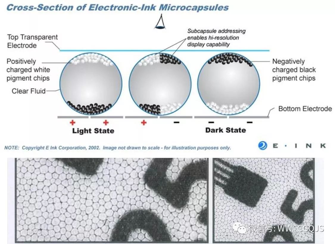
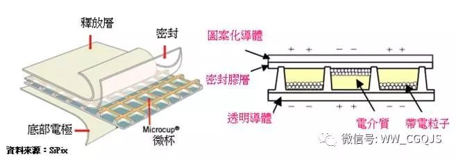
Electrophoretic display (EPD) is a new display technology that uses electrophoresis to move charged substances sandwiched between electrodes under the action of an electric field and alternately display two or more different colors by the movement of charged substances. . Taking one electrophoresis unit as one pixel, the electrophoresis unit is arranged in a two-dimensional matrix to form a display plane, and pixels can display different colors according to requirements, and a combination can obtain a planar image.
Schematic diagram of E-Ink microcapsule electrophoresis technology

Schematic diagram of SiPix Microcup electrophoretic display technology
Cholesterol electronic paper technology
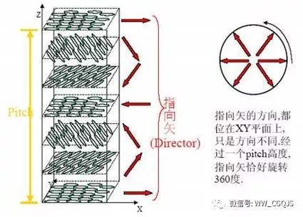
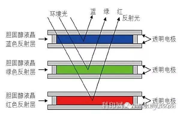
The cholesteric liquid crystal is mainly formed by multi-layer nematic liquid crystal (nematic) deposition, and the addition of an optically active liquid crystal molecule (chiral molecule) in the multilayer nematic liquid crystal causes the long-axis direction of the molecules of the multilayer nematic liquid crystal layer. Gradually, the angle is rotated to form a spiral shape. This structure is similar to cholesterol molecules, so it is called a liquid crystal of cholesterol.
Electrowetting electronic paper technology
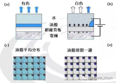
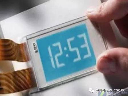
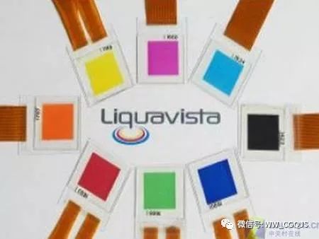
Flexible OLED display technology
working principle
Flexible OLED (FOLED) display is the use of OLED technology to fabricate display devices on flexible plastics or metal films. The basic structure is "flexible substrate / ITO anode / organic functional layer, metal cathode", light-emitting mechanism and ordinary glass substrate OLED is similar. Flexible (FOLED) devices are typically formed on a glass or polymer substrate consisting of a transparent anode, a metal cathode, and two or more organic layers sandwiched between them. When a forward voltage is applied to the device, under the action of an external electric field, holes and electrons are injected into the organic small molecule and the polymer layer from the positive electrode and the negative electrode, respectively, and the oppositely charged carriers are in the small molecule and the polymer layer. The migration, recombination in the luminescent layer, forms excitons. The excitons transfer energy to the luminescent molecules, exciting the electrons to the excited state, and the excited state energy is deactivated by radiation to generate photons to form luminescence. The basic structure of the organic electroluminescent device is a sandwich structure, that is, each organic functional layer is sandwiched by the electrodes on both sides like a sandwich, and at least one of the electrodes is transparent to obtain surface illumination, as shown in FIG. Specifically, the basic device structure of the OLED has a single layer, a double layer, a three layer, and a multilayer.
Since the mobility of electron holes in the organic thin film is different, resulting in unbalanced charge injection, the luminous efficiency is lowered. Therefore, a multilayer device structure is generally employed: a substrate/anode/hole injection layer. (hole injection layer) / hole transport layer / electron transport layer / cathode. Evaluation of the flexible OLED can be evaluated from two aspects of the luminescent properties of the luminescent material and the electrical properties of the device. The illuminating performance mainly includes the emission spectrum, luminous efficiency and lifetime, etc. For the visible light of the display device, there are parameters such as illuminating brightness and illuminating chromaticity, and electrical properties such as current and voltage.
In addition to the substrate, the flexible display device also requires a flexible transparent electrode, and a flexible display driving circuit to achieve control of the display member. At present, electronic materials based on rigid matrix-silicon cannot meet this requirement.
Carbon nanotubes, graphene, etc. can be used as conductors, semiconductors, and even insulators by a suitable treatment. More importantly, these two nano-carbon materials can still guarantee the operation of their devices under flexible service conditions (closely related to their good mechanical strength and elasticity). Therefore, the use of carbon nanotubes and graphene to prepare flexible circuits has become a trend.
Flexible circuit
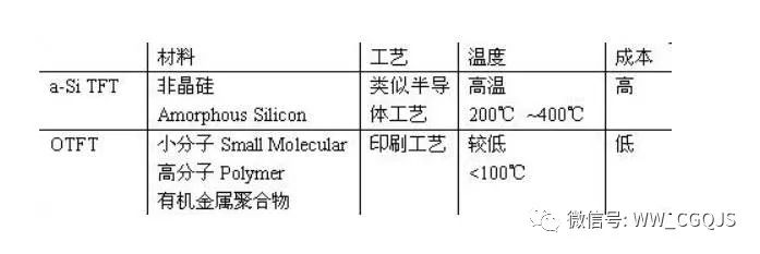
OTFT (Organic Thin Film Field Effect Transistor) is used instead of TFT. This transistor has better flexibility and is similar to the thermal expansion coefficient of polymer substrate. It is suitable for low temperature process and can be mass-produced by inkjet printing technology, which reduces the cost.
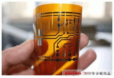
Carbon nanotubes, graphene, etc. can be used as conductors, semiconductors, and even insulators by a suitable treatment. More importantly, these two nano-carbon materials can still guarantee the operation of their devices under flexible service conditions (closely related to their good mechanical strength and elasticity). Therefore, the use of carbon nanotubes and graphene to prepare flexible circuits has become a trend.
Flexible integrated circuit for carbon nanotube preparation
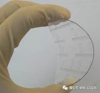
a transistor in which a carbon nanotube is a semiconductor material
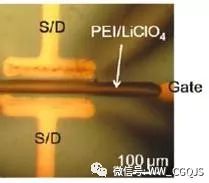
Display device integrating OLED and carbon nanotube transistors at the same time
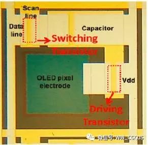
Flexible electrode
Flexible transparent conductive film made of graphene
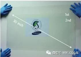
Flexible thin film battery
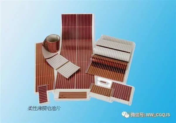
Microscopic morphology of carbon nanotube flexible transparent conductive film
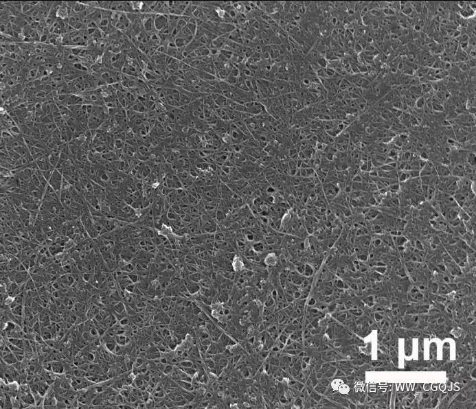
The most basic function of the transparent electrode: as a component of the light-emitting circuit (conducting), providing a light-emitting window
At present, the preparation of the transparent electrode mainly uses an indium tin oxide film material, but its flexibility is limited.
In contrast, carbon nanotubes and graphene have high transparency and high electrical conductivity, and are one of the alternative materials for indium tin oxide materials.
Preparation Process
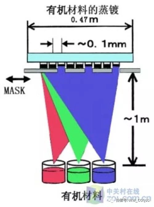
Vacuum evaporation
High environmental requirements. The process must be carried out in a vacuum chamber, requiring a visor to be placed next to the glass substrate to determine the pattern of deposited material on the substrate.
It is difficult to make large sizes. Vacuum thermal evaporation technology is relatively easy when producing small screens, but it is difficult to make large screens. The visor is highly susceptible to offset by the high temperature environment in the process, making it difficult to maintain a uniform deposition rate on a large substrate.
The cost is too high. The complexity of the process, the special environment, and the low yield rate have caused the price of OLED screens to remain high at this stage.
Inkjet printing
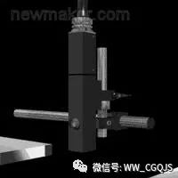
Can be enlarged. Using inkjet imaging technology, the same on-demand inkjet process as the inkjet printer can be used to accurately deposit the organic material in the desired amount, allowing the organic material to be uniformly deposited to form a thin film layer, which can effectively solve the large size. The manufacturing problem of OLED screens.
cut costs. The inkjet system has a very high utilization rate of materials, and manufacturers can reduce production costs.
Simplify the production process and facilitate mass production. This production process eliminates the need for a visor and reduces process steps, which can significantly increase throughput.
Non-contact printing eliminates contact contamination of functional materials
Roll-to-roll
Asic Miner Bitmain:Asic Miner Bitmain Ka3 166Th Kda Mining Machine
Bitmain is the world's leading digital currency mining machine manufacturer. Its brand ANTMINER has maintained a long-term technological and market dominance in the industry, with customers covering more than 100 countries and regions. The company has subsidiaries in China, the United States, Singapore, Malaysia, Kazakhstan and other places.
Bitmain has a unique computing power efficiency ratio technology to provide the global blockchain network with outstanding computing power infrastructure and solutions. Since its establishment in 2013, ANTMINER BTC mining machine single computing power has increased by three orders of magnitude, while computing power efficiency ratio has decreased by two orders of magnitude. Bitmain's vision is to make the digital world a better place for mankind.
Asic Miner Bitmain,Ka3 166Th Kda,Kda Miner Antminer Ka3,Asic Miner Ka3,ka3 miner
Shenzhen YLHM Technology Co., Ltd. , https://www.asicminer-ylhm.com
