The content stored in memory can be programs or data. The program is the instruction code that the ARM processor can run, and the data is the operand or variable used by the instruction in the operation.
1, program storage
The ARM processor supports two kinds of instructions, one is an ARM assembly instruction and the other is a Thumb assembly instruction. The ARM assembler instruction is 32 bits long, that is, each ARM assembler instruction is stored by four bytes of memory, so the ARM processor will fetch an instruction from the address a + 4 when executing the ARM assembler instruction at address a. . The Thumb assembler instruction is 16 bits long. That is, each Thumb assembler instruction is stored with two bytes of memory. Therefore, when the ARM processor executes the Thumb assembler instruction at address a, it fetches the next instruction from address a + 2. .
ARM processors can execute instructions in two formats. Running assembler instructions in different formats can make a big difference in execution and instruction fetching. In order to distinguish, ARM kernel can work under two working conditions.
l ARM state 32-bit word-aligned ARM assembler instructions are now executed. In this state, the ARM processor stores, reads, or executes instructions in a single word (ie, 32 bits) as the basic unit;
l THUMB state 16-bit half-word-aligned Thumb assemble instructions are now executed. In this state, the ARM processor stores, reads, or executes instructions with a half-word (ie, 16-bit) base unit;
l These two operating states can be converted, but the conversion does not affect the processor state and register contents.
2, data storage
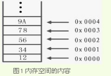
ARM processors support three data lengths for data operations (read or write): byte (8 bits), halfword (16 bits), and word (32 bits). Assuming that the data shown in Figure 1 is stored in the memory space at addresses 0x0000 to 0x0004, we will read data from the memory space in three data sizes. (Assume that the data storage format is little-endian storage format)

Figure 1 The contents of the memory space
l byte: take a byte of data from the address 0x0000, then take out the content of 12; take a byte of data from the address 0x0001, then take out the content of 34;
l half-word: take a half-word data from the address 0x0000, then take out the content is 3412; take a half-word data from the address 0x0001, then take out the content is 5634;
l Word: Takes a word data from the address 0x0000, then take out the content is 78563412; Take a word data from the address 0x0001, then take out the content is 9A785634.
It should be noted that the ARM processor has to be aligned with the data when it operates, and it is necessary to find the correct address. When operating on 16-bit data, the last bit (0) of the address data should be 0. When operating on 32-bit data, the last two bits (1:0) of the address data should be 0. For example, when operating on a word, the ARM processor does not allow a word to be read from address 0x0001.
Nowadays, ARM versions do not support non-aligned word transfers (ARMv3, ARMv4, ARMv5). In ARMv6, the transfer of non-aligned words began to be supported.
3, "von Neumann" architecture and "Harvard" architecture
When it comes to ARM programs and data storage, we should talk about the "von Neumann" architecture and "Harvard" architecture. Because ARM7 series adopts von Neumann architecture, and ARM9~ARM11 adopts Harvard architecture. The two structures are described as follows:
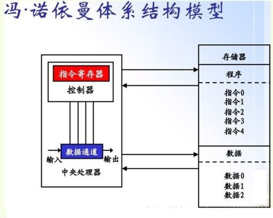
"Von Neumann" architecture
In the mid 1930s, the German scientist von Neumann boldly proposed to abandon the decimal system and use binary as the digital system basis of digital computers. At the same time, he also said that the computer program is pre-programmed and then the computer performs numerical calculations in accordance with the order of calculations made beforehand by people.
The main point of von Neumann's theory is that the number system of digital computers adopts binary numbers; computers should be executed in program order.
Its main content is:
l The computer consists of five parts: the controller, the operator, the memory, the input device, and the output device.
l Programs and data are stored in memory in binary code indiscriminately, and the storage location is determined by the address.
l The controller operates according to the sequence of instructions (programs) stored in the memory and is executed by a program counter control instruction. The controller has the ability to judge and can select different workflows based on the calculation results.

Harvard architecture
Digital signal processing generally requires a large amount of computation and a high speed of operation. In order to improve data throughput, Harvard architecture is mostly used in digital signal processors.
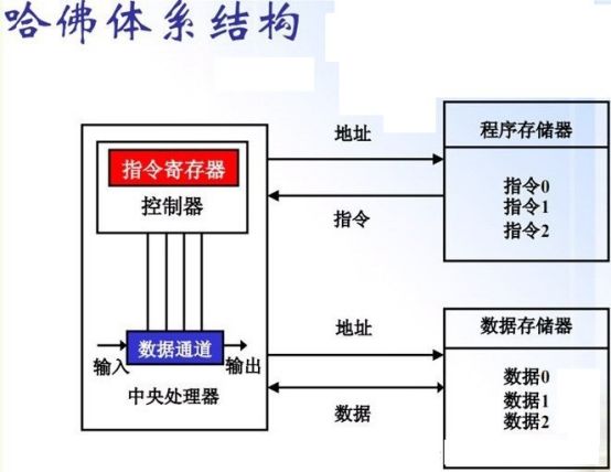
Harvard structure features are as follows:
l Use two independent memory modules to store instructions and data, and each memory module does not allow coexistence of instructions and data in order to achieve parallel processing;
l It has an independent address bus and an independent data bus. It uses public address bus to access two storage modules (program storage module and data storage module). The common data bus is used to complete the program storage module or data storage module and CPU. Data transfer between;

Two structural differences
In a typical case, completing an instruction requires three steps, namely: fetching an instruction, decoding an instruction, and executing an instruction. From the timing relationship of instruction flow, we can also see the difference between Von. Norman structure and Harvard structure processing.
Give a simplest instruction to read and write to memory. Instruction 1 to instruction 3 store and fetch instructions. For Von Norman architecture processors, instructions are fetched and data is accessed from the same memory space. Take, transfer via the same bus, so they can not be executed in an overlapping manner, only one completes before proceeding to the next.
If the Harvard architecture is used to handle the same three access number instructions, as shown in the figure below, since the instruction fetches and accesses data via different storage spaces and different buses, each instruction can be executed in an overlapping manner. It overcomes the bottleneck of data stream transmission and improves the speed of operation.
Innosilicon Machine:Innosilicon A10 ETHMaster (500Mh),Innosilicon A10 Pro ETH (500Mh),Innosilicon A10 Pro+ ETH (750Mh),Innosilicon A11 Pro ETH (1500Mh)
Innosilicon is a worldwide one-stop provider of high-speed mixed signal IPs and ASIC customization with leading market shares in Asian-Pacific market for 10 consecutive years. Its IP has enabled billions of SoC's to enter mass production, covering nodes from 180nm to 5nm across the world`s foundries including: GlobalFoundries, TSMC, Samsung, SMIC, UMC and others. Backed by its 14 years of technical expertise in developing cutting-edge IPs and ASIC products, Innosilicon has assisted our valued partners including AMD, Microchip and Microsoft to name but a few, in realizing their product goals.
Innosilicon team is fully devoted to providing the world's most advanced IP and ASIC technologies, and has achieved stellar results. In 2018, Innosilicon was the first in the world to reach mass production of the performance-leading GDDR6 interface in our cryptographic GPU product. In 2019, Innosilicon announced the availability of the HDMI v2.1 IP supporting 4K/8K displays as well as our 32Gbps SerDes PHY. In 2020, we launched the INNOLINK Chiplet which allows massive amounts of low-latency data to pass seamlessly between smaller chips as if they were all on the same bus. With a wide range of performance leading IP in multiple FinFET processes and 22nm planar processes all entering mass production, Innosilicon's remarkable innovation capabilities have been proven in fields such as: high-performance computing, high-bandwidth memory, encrypted computing, AI cloud computing, and low-power IoT.
Innosilicon Machine,A11 Pro 1500M Miner,Asic Miner A11 Pro 8G,A11 Pro 8G 1500Mh,ETC miner
Shenzhen YLHM Technology Co., Ltd. , https://www.ylhm-tech.com
