The emergence of system-on-chip allows the chip to achieve more complex functions and achieve higher performance, but at the same time its internal signals become more and more difficult to observe and control, and the corresponding test and debugging work also encounters insurmountable time complexity. difficult. The International Semiconductor Technology Roadmap for Semico nducto rs (IT RS) points out that the time required for debugging and locating problems will grow exponentially as the process progresses. Due to the complexity of the testing and commissioning work, the cost is often higher than the design cost, which is about 1 / 3 of the total design cost of the entire SoC. Throughout the SoC hardware design process, from the first shot to the final successful implementation of all functions, hardware debugging time is close to 35% of the entire time, and this number will increase with the increase of integration.
In the entire system-on-a-chip, the microprocessor is the core and the most complex module, so the providers of each processor core have invested a lot of research and development, and integrated rich debugging functions in their cores. Most of today's popular debugging techniques use the debugging scheme of JT AG. However, this method generally inserts a scan chain inside the target system. When the processor works at high speed, it will inevitably limit the performance of the processor.
To this end, the design proposes a new debug structure that does not rely on the JTA G interface and requires less pin overhead. It monitors the on-chip communication status in real time by attaching it to the on-chip high-speed bus, and it directly performs with the processor. The interaction can control the processor and access all the on-chip storage units without affecting the normal operation of the processor. The user can perform remote debugging through a dedicated data output link, issue debugging instructions and obtain feedback information. Combined with the above characteristics, the design will take the three basic features required for a good debugging structure proposed in the literature [3] as the design starting point: the observability of debugging; the controllability of debugging; efficient communication efficiency; low intrusion Sex.
1 Debug system composition
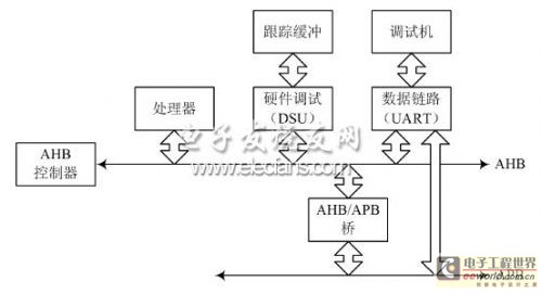
The hardware debugging module DSU is the core, the AMBA 2.0 bus is the architecture, and the system structure of the dedicated UART is the debug link interface as shown in Figure 1.

Figure 1 Debug system structure
The debugging host issues a debugging instruction to the debugging unit through the bus interface U ART; the debugging unit will control the debugging state of the system, and when the trigger condition is met, the processor will be suspended by direct communication with the processor, and the user can use the debugging host to debug the interface. Access all memory locations on the chip to obtain system status information. The bus trace buffer can work in two modes. In normal mode, the bus communication status is recorded in real time through the DSU. In the debug mode, it is accessed by the debug host to find the problem. The root cause of the occurrence; the instruction trace cache is inside the microprocessor to store the executed instructions; the debug interface UART will provide a protocol conversion service between the debug host and the bus to realize the mutual conversion of serial data and parallel data.
1. 1 AHB bus
In SoC design, the design of the internal bus of the chip often determines the performance, power consumption and complexity of each module. The bus is usually selected based on two aspects: one is the inherent needs of the chip design process, and the other is the need for switching bandwidth, latency, and efficiency flexibility. The design uses an on-chip high-speed bus protocol AHB proposed by ARM, which has the following features: Support for burst transmission; Support for block transfer; Single-cycle bus control transfer; Single clock edge operation; Non-tri-state execution; Wide data Bus architecture; data and address streams overlap. In addition, the protocol supports static timing analysis and friendly test insertion.
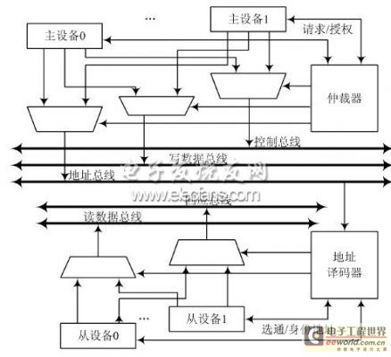
The AHB structure of the system design is shown in Figure 2. It consists of a master-slave module, an arbiter, and an address decoder, and uses a central multiplexer interconnect. As a core component, the arbiter receives the bus request of up to 16 master devices. In order to realize the design intention of configurable!, the partitioning-based arbitration strategy is adopted to implement two fixed and polling priority algorithms, which can be flexibly selected by users. . The centralized address decoding mechanism adopted by AHB is beneficial to improve the portability of peripheral devices. The central decoder decodes the address sent from the address bus and the identity information of each slave to select the slave device. The design is designed to reduce The logic is calculated and the power consumption is reduced, and only the high-order bits of the address are discriminated. The entire AHB system is connected by a multiplexer, which avoids the power consumption, speed and testability problems caused by the tri-state bus. The control signals and address data required by the system will be routed by the multiplexer to the corresponding The destination device can divide the multiplexer into a multiplexer from the master multiplexer and the slave module to the master module according to the direction of the route. In addition, in order to solve the problem of bus parking when there is no host request bus, the system also designs a default master whose default host number depends on the selected arbitration algorithm. Split transmission is a prominent feature of AHB. It plays an active role in preventing system deadlock and making full use of the bus. Here, in order to solve the problem of split locked and address miss, the design implements a A virtual slave device, when the above problem occurs, the virtual slave device will send a response signal on its behalf.

Figure 2 AH B bus system interconnection structure
Electronic Cigarette,Largest E-Cig Oem,China E-Cig Oem,Vape Pen Oem,Vape Device Oem
Shenzhen MASON VAP Technology Co., Ltd. , https://www.masonvap.com
