
Abstract: For the vibration monitoring of mechanical equipment operation, the vibration signal acquisition system is designed, and a design scheme of vibration signal acquisition system based on FPGA is proposed. The system hardware structure, signal conditioning circuit and data acquisition module are designed. The control logic of A/D sampling is discussed. The experimental verification shows that the system can achieve a sampling rate of 10 K per second and an acquisition accuracy of 16 bits, which can meet the requirements of real-time and accuracy.
With the development of high-speed, high-efficiency, high-precision and large-scale production machinery, transportation machinery or engineering structure, failure of any component of mechanical equipment may reduce processing accuracy, bring greater economic losses, and even endanger personal safety. Vibration condition monitoring of mechanical components has become an indispensable part of production, and early failure prediction of the corresponding mechanical components. In this paper, the FPGA is used as the core to develop the vibration signal acquisition system, and the data acquisition module and communication module are synchronously designed.
1 overall designThe vibration signal acquisition system takes the FPGA chip as the core, collects the vibration signal through the A/D conversion chip, and then transmits the collected data to the upper computer through the RS-422 serial bus interface, and makes corresponding diagnosis processing in the fault diagnosis software. The hardware of the vibration signal acquisition system can be divided into signal conditioning circuit, A/D conversion circuit, FPGA control logic and RS-422 interface conversion circuit according to the function module. The hardware structure of the system is shown in Figure 1.
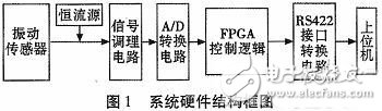
The functions of each functional module of the system hardware are as follows:
1) Signal conditioning circuit: the signal conditioning circuit is mainly pressed by the integrated circuit
The vibration signal collected by the Integrated Circuit Piezoelectricity (ICP) accelerometer is subjected to conditioning drive, amplification and anti-aliasing filtering, so that an analog to digital converter ADC chip can acquire the vibration signal and further Processing work.
2) A/D conversion circuit: The A/D conversion circuit performs analog-to-digital conversion on the signal-conditioned signal, and transmits the conversion result to the FPGA for data acquisition. This function circuit determines the resolution and acquisition accuracy of the entire system.
3) FPGA control logic: The FPGA chip is the core part of the main control module, which controls the acquisition and data transmission of the vibration signal. This function circuit controls the sampling period of the system.
4) RS422 interface conversion circuit: The digital signal after A/D conversion is transmitted to the host computer through the RS422 bus.
2 hardware circuit design2.1 constant current source circuit
The system uses ICP integrated circuit piezoelectric acceleration sensor to detect the vibration signal of the device under test. It integrates the traditional piezoelectric acceleration sensor and amplifier. The power supply and signal output share the same cable, and it is powered by the constant current source. After the signal conditioning circuit is connected to the single-chip microcomputer for testing, the acquisition system is simplified, the number of cables is reduced, and the charge amplifier is omitted, thereby reducing the cost.
The power supply required for the ICP sensor must be capable of supplying a DC voltage of 18 to 30 V and a constant current of 2 to 20 mA. Since the sensor shares the power line and the signal output line, its output signal will contain a DC bias voltage of 8 to 14 V, and the DC component of the signal is filtered by a decoupling capacitor.
This system uses TI's three-terminal adjustable constant current source device LM334 chip. LM334 is a single-chip three-terminal adjustable constant current source. In practical applications, changing the connection resistance can constitute an ideal current floating source without independent power supply. Changing R can change the current value of the constant current source. The formula is:
The system is set to an operating voltage of 28 V for the LM334, a nominal R of 33 Ω for the resistor R, and an output current of 2 mA.
2.2 Signal Conditioning Module Design
2.2.1 Isolation and amplification circuit design
The output signal of the ICP accelerometer includes a DC bias voltage. The circuit design separates the DC component by the DC capacitors C1 and C2, and then uses a precision instrumentation operational amplifier chip to amplify the analog signal. The gain can be achieved by adjusting the external proportional resistor. Any choice between 1 and 10 000. The schematic diagram of the isolation and amplification circuit is shown in Figure 2.
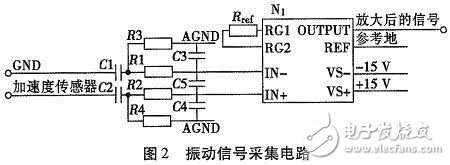
N1 is a precision instrumentation operational amplifier, and its gain value can be calculated according to the following formula:
Where: G is the voltage amplification gain; Rref is the proportional reference resistance in Ω.
At this stage, the Rref is opened, that is, Rref=∞, and the calculation shows that G=1.
R1 and R2 are input matching resistors with a nominal value of 4.7 kΩ.
R3 and R4 are open circuit grounding resistors with a nominal value of 1 MΩ.
C1 and C2 are DC blocking capacitors at the input end. The nominal value is 0.1μF and the rated voltage is 50V. Through the high-pass circuit composed of C1, C2 and R3, R4, the -3 dB cut-off frequency is 15.92 Hz, and the signal is directly blocked without affecting the acquired signal.
C3, C4, and C5 are the filter capacitors at the input of the precision instrumentation operational amplifier. The nominal values ​​are 0.001μF, 0.01μF, and 0.001μF. They form a low-pass circuit with R1 and R2. The -3 dB cutoff frequency for the common-mode signal is 33.87. kHz, the -3 dB cutoff frequency for the differential mode signal is 1 610 Hz, effectively filtering out the interference signal entering the acquisition circuit.
2.2.2 Anti-aliasing filter circuit design
The amplified vibration signal will be mixed with high-frequency interference signals, and these high-frequency signals will cause frequency aliasing, which will cause the accuracy of the acquisition system to decrease.
The anti-aliasing filter circuit uses a second-order voltage-controlled voltage source low-pass filter circuit, and the cutoff frequency of the filter is controlled by resistors R1, R2 and capacitors C1 and C2. The schematic diagram of the second-order low-pass filter circuit is shown in Figure 3.
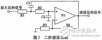
The filter circuit design parameters are as follows:
R1=R2=15 kΩ, R3=R4=10 kΩ, C1=C2=10nF;
The transfer function of the second-order low-pass filter circuit is:
Where: A(s) is the open-loop gain; Q is the equivalent quality factor; ωn is the characteristic angular frequency s of the circuit.
Among them, Avf=1+R3/R4=2, Q=1/(3-Avf)=1>0, so the poles of A(s) are all located in the left half s plane, and the circuit does not generate self-excited oscillation.
On the other hand, the amplitude-frequency response expression obtained by the filter circuit transfer function is:
It can be calculated that when ω/ωn=10, the amplitude-frequency characteristic curve has a -40 dB attenuation, and the amplitude-frequency response of the circuit has better low-pass characteristics. The filter cutoff frequency f=1/2πRC≈1 062 Hz .
2.3 Design of data acquisition module
The data acquisition module is mainly designed around the A/D conversion chip. The system selects a single-channel 16-bit A/D conversion chip for sampling, and the sampling frequency is up to 100 ksps. The frequency of the vibration signal of the target sample is generally a low frequency signal. The vibration signal of the 5 kHz frequency range is designed by the acquisition system. According to the Shannon sampling theorem, the acquisition rate of the A/D conversion chip should be no less than 10 k per second, 100 ksps. The A/D converter chip can fully meet the needs of this system.
Since the output level of the A/D converter chip is 5 V TTL level, it is necessary to configure a level conversion chip to convert the 5 V level to a 3.3 V level and then to the Field Programmable Gate Arrays (FPGA). ), completes the timing control of the A/D conversion chip in the acquisition circuit.
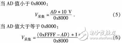
A/D conversion formula: The 16-bit binary number collected by the A/D chip is 0~0xFFFF, corresponding to the voltage of -10 V to +10 V. The voltage conversion calculation formula is as follows:
2.4 Design of communication module
The RS-422 driver circuit consists of a UART protocol, level shifting, and interface circuitry, where protocol conversion is implemented by programmable logic. The serial interface data format is: 1 start bit, 8 data bits, odd parity bit, 1 stop bit, and the operating frequency is designed at 115 200 bps. The FPGA chip forwards the acquired AD converted data to the RS-422 bus. Since the AD acquisition chip is 16 bits, the upper 8 bits of the pre-transmit data are set, and the lower 8 bits of the data are transmitted.
Electrical Products,Upvc Pipe Fitting,Pvc Pipe Fittings,Pipe Fitting Flange,Pipe Clamp Fitting
FOSHAN SHUNDE LANGLI HARDWARE ELECTRICAL CO.LTD , https://www.langliplastic.com