The integrated circuit IC1 is a timer, the output frequency is determined by the peripheral timing components R2 and C1, and the timing pulse outputted by the 3-pin is sent to the clock input terminal of the counter IC2. IC2 is connected into a six-way circuit, and the pulse train input from IC1 to the IC2CLK terminal is sequentially allocated to the Q0 to Q5 terminals of IC2. The transistors V1 to V5 are used to charge the capacitors C3 to C7, respectively, and the transistors V6 and V7 discharge the five capacitors C3 to C7 that have been charged. Since the voltages charged on C3-C7 are equal, a DC voltage of about 5 times the original charging voltage is obtained at the discharge output. The operating voltage of this circuit is provided by two parts:
The operating voltage of IC1 and IC2 is 9V, and the current consumption is very small. The other part can supply C~C7 charging voltage of 3~12V, and the DC voltage of about 15-50V can be obtained at OUT. Therefore, you can select the corresponding one according to your needs. The operating voltage gets the desired output voltage.
In the process of counting and outputting the IC2 from the Q0 to the Q5 terminals in sequence, V1 to V5 are sequentially gated, and the capacitors C3 to C7 respectively supply charging currents through the diodes D1 to D5, and sequentially charge C3 to C7. When the JC2 count is output to the Q5 terminal, V6 and V7 are both turned on, and the power supply is superimposed with the voltage on the charged C3 to C7 through the ce junction of V7, so that the DC terminal of the circuit obtains a DC voltage of about 5 times the charging voltage. . Since IC2 counts one cycle, capacitors C3 and C7 are charged and discharged once, and the OUT terminal of the circuit outputs a pulse. Therefore, when IC2 is continuously output, continuous pulse output can be obtained at the OUT terminal. After smoothing and filtering by the storage capacitor c8, it is continued. , stable DC voltage. It can be seen that the higher the counting frequency of IC2, the smoother the voltage obtained at the OUT terminal. Therefore, the output voltage characteristic of the OUT terminal can be improved by appropriately changing the operating frequency of IC1.
The circuit is as shown
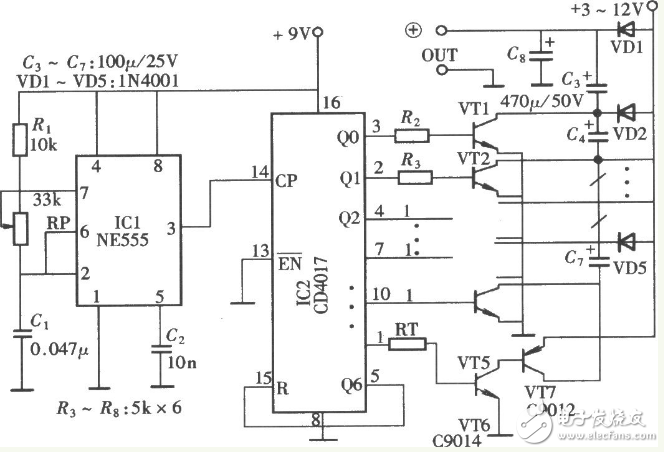
This circuit is a five-fold voltage output type, but it can also be set to 2-8 times voltage type according to the need. When connecting, IC2 can be set to 2~8 frequency dividing circuit, and 2~8 capacitors are sequentially charged through each triode. The voltage from each capacitor is discharged by the last transistor, and the voltage output of any voltage is obtained at the OUT terminal. When the output voltage of the OUT terminal is high, the withstand voltage of C3~C8 should also be increased accordingly, especially C8. In order to avoid breakdown.
In the figure, the transistors V1 to V5 are preferably Darlington transistors, and the resistance is 1/8W carbon film resistance. The 9V voltage for lC operation in the figure can be provided by a 9V stack battery, and the voltage of the voltage doubled can be provided by other power sources. Circuit fabrication and debugging Two ICs can be installed using the lC socket. The current consumption of the lC should be minimized under normal IC operation. The polarity of each charging capacitor cannot be reversed. After the production is completed, the power can be tested after careful inspection. This circuit can work normally after power-on, generally no debugging is required. This circuit can also be used for DC boosting of the internal power supply.
Electronic voltage doubler and boost circuits have unique advantages in some portable electronic instruments because they eliminate the step-up transformers used in conventional boost circuits and replace them with integrated circuits and capacitors. This can reduce the weight of the instrument, and can also improve the conversion efficiency of the power supply. The circuit composition is shown in the figure. The circuit consists of a pulse oscillator, a pulse divider, a transistor switching circuit, a storage capacitor and an isolation diode.
DC double voltage boost circuit diagram (2)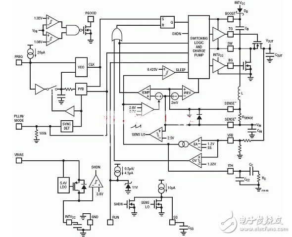
The LTC3786 is a high efficiency synchronous boost power controller that does not require a heat sink. The VIN input voltage ranges from 4.5V to 38V. The operating voltage is as low as 2.5V after startup. The output voltage is up to 60V and the reference voltage is 1.2V ± 1%. Synchronous MOSFET with 100% duty cycle capability, quiescent current 55? A, mainly used in industrial and automotive power supplies, automotive starting systems, medical equipment and high-voltage battery-powered systems.
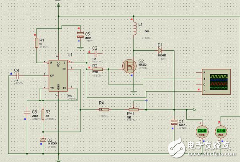
DC double voltage boost circuit diagram (3)At the instant of 1.5V turn-on, the 1.5V DC voltage charges C2 through the energy storage inductors L and R1. Since the voltage across the capacitor cannot be abrupt, the VT1 base voltage is almost zero, so VT1 is turned on, which makes VT2 saturating. At this time, the current of L will gradually increase from small, and L converts the electric energy into magnetic energy for storage. In this process, VD2 is cut off, Vo=0V, and the voltage regulator circuit composed of VT3, R2, VD3, and VD1 does not work. 2 When the current in L no longer changes, the base potential of VT1 also increases to the maximum. At this time, VT1 turns on and turns off, and VT2 also cuts off. Since the current flowing through L cannot be abrupt, L ends will produce a reverse The phase induced electromotive force UL has a polarity of left negative and right positive. This UL is connected in series with 1.5V DC to increase the voltage of the VT2 collector to ground. At this time, VD2 is turned on. When Vo is greater than 9V, VT3 is turned on, and Vo is turned on. High, the higher the voltage applied to the base of VT1 through VT3, the smaller the conduction angle of VT1, the smaller the conduction angle of VT2, and the lower the current flowing through L, thus controlling the energy storage of L. Therefore, the Vo dynamic stability is achieved at a certain voltage value (9V).
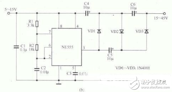
Road working process: In Figure (a), after the power is turned on, the power supply first charges C4 through VD1, so that the voltage across c4 is close to the power supply voltage. When the rising edge of the NE555's 3-pin output pulse, charge C4 again. According to the principle of rising water, the voltage of C4 positive pole to ground reaches: power supply voltage + pulse peak voltage. This voltage is then charged to C5 via VD2, causing the C5 positive to ground voltage to reach C4, which is equal to twice the supply voltage. When the falling edge of the pulse comes, the power supply is again charged to C4 through VD1, and the above process is repeated.
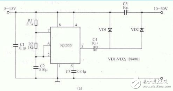
Figure (b) shows a 3x voltage boost circuit. As can be seen from the figure, the boost circuit of the circuit is composed of three sets of diode-capacitor circuits. If it is connected with the connection of Figure 2-42 (a), it will be found that the components added by this circuit are The position comparison is VDl and c4. In this circuit, each of the three sets of diode-capacitor circuits can increase the output voltage of the previous stage by one supply voltage. Three sets of such circuits can increase the output voltage to three times the supply voltage. Figure 2-42 (c) shows a 4x voltage boost circuit consisting of 555 circuits consisting of 4 diode-capacitor circuits that ultimately increase the output voltage to four times the supply voltage.

As shown in the figure, the circuit diagram of the CD4069 voltage boosting power supply.
The voltage doubler boost circuit composed of the gate circuit can provide the required high voltage working power for some electronic devices. Although the output current is not large enough, it is an economical and convenient power source for some circuits that require a sufficiently high voltage without requiring a large current.
Orange Enzyme Into Beauty Revitalizing Mask 2
Remove dirt and excess oil within the pores, and remove aging skin, making skin fresh and clean. Mask hydrating agent, will lock the moisture in the membrane, soften cuticles and help the skin to absorb nutrients, Mask quickly soothe the skin, eliminate fatigue and restore the skin's luster and elasticity. Pristine liquid containing plant extracts to soften skin tissue, promote skin metabolism, for dry or dehydrated skin. White Water mask can thoroughly remove dead skin cells, while having clean water and instant whitening effect, make the skin smooth and reproduce young, white and transparent.
Companies registered capital of 35 million yuan, the end of 2014 the total assets of 48.69 million yuan, including fixed assets of 37.52 million yuan. The company's existing cooperation Orange cultivation base 7043.5 acres, the company production base is located in Jiangxi County Tech Industrial Park Chu Tan industrial area, covers an area of 120 acres, it has built a standard plant 9,000 square meters, Nissan 6000 kg Orange enzymes and other liquid enzyme products. Enzyme, known as enzyme, refers to a polymer substance having biocatalytic functionality. In the catalytic reaction system an enzyme, the reactant molecules are known as substrates, enzyme substrates by catalytic conversion to another molecule. Almost all cellular activity of enzymes involved in the process are required to improve efficiency. Similar to other non-biological catalysts, enzymes chemical reactions by lowering the activation energy to accelerate the rate of the reaction, most of the enzyme catalyzed reaction rate can be increased a million times; in fact, the enzyme is to provide an activation energy needs than another low way, so that more particles to have less than the activation energy of the reaction kinetic energy, thus speeding up the reaction rate. Enzyme as a catalyst, in itself is not consumed during the reaction, it does not affect the chemical equilibrium reactions. Positive enzyme catalysis, but also a negative catalytic effect, not only to accelerate the reaction rate, but also to reduce the reaction rate. And other non-living catalysts is different, having a high degree of specificity of enzyme, only a catalytic reaction or produce a particular specific configuration.
White Water Enzyme Mask,Removal Aging Skin Enzyme Mask,Rapidly Relieve Skin Enzyme Mask
guangdong ganzhou ningbo , https://www.tlqcjs.com
