
Full complement transistor power amplifier fabrication circuit
Most beginners are more enthusiastic about the fabrication of integrated circuits because of their higher success rate. However, the integrated power of the integrated IC and the discrete component circuit of the same power are obviously lacking in dynamics.
The production of discrete component amplifiers is actually not difficult to succeed as long as the materials are carefully selected. The power amplifiers described below do not need to be debugged, which is worthy of imitation.
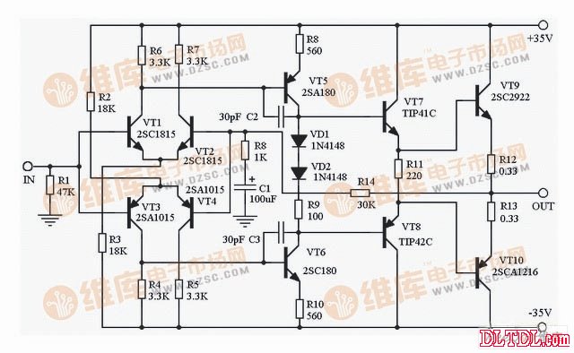
This is an OCL power amplifier circuit that uses a fully complementary symmetrical circuit drive method. It is a circuit that is used more in the mid-range power amplifier. It has good symmetry, wide frequency response and simple structure. Although the distortion is not particularly low (about 0.03%), the dynamic index of the circuit's conversion rate and TIM distortion is quite good. Therefore, the sound quality is very good, and it is currently the preferred circuit for making high-fidelity power amplifiers for home use. The first stage of the circuit uses complementary symmetrical differential circuits. The static working current of each tube is about 1mA. The high-quality low-noise complementary tubes 2SC1815 and 2SA1015 are used as complementary differential pair tubes, which have low noise and high dynamic range. The second stage voltage amplification uses a complementary push-pull circuit, using high complementary pairs of tubes A180, C180, operating current of about 5mA, diodes and resistors connected in series with the two tubes to provide a bias voltage of about 1.6V for the buffer stage. Two complementary* rate pairs of tubes TIP41C and TIP42C form the emitter follower buffer driver stage. Adding the emitter follower buffer driver stage is one of the main features of modern OCL circuits. Its main voltage amplification stage has high load impedance and is stable. Higher gain. At the same time, it provides a lower output internal resistance for the output stage, which accelerates the charging speed of the output junction capacitor Cbe to improve the transient characteristics and frequency characteristics of the circuit. The operating current of this stage is also large, generally (10-20) mA, and even up to 100 mA for individual models, which is similar to the quiescent current of the output stage, so that the output stage can be fully driven. Its emitter resistance is suspended (not centered), which forces the stage to be fully Class A and provides a bias voltage for the output stage. The output stage is a traditional complementary OCL circuit, which uses a triple-power complementary pair C2922, A1216 with FT up to 60MHz, and a quiescent current of about 100mA. The output is connected to the inverting input of the input stage with a loop negative feedback network and the circuit gain is set to 31 times.
SHENZHEN CHONDEKUAI TECHNOLOGY CO.LTD , https://www.szfourinone.com