Appliances such as power tools, gardening tools, and vacuum cleaners are driven by a low-voltage (2 to 10 knots) lithium-ion battery-powered motor. These tools use brushed direct current (BDC) or three phase brushless direct current (BLDC) motors. BLDC motors are more efficient, less maintenance, less noisy and longer lasting.
The most important performance requirements for the drive motor power stage are small size, high efficiency, good heat dissipation, reliable protection, and high peak current carrying capacity. The small size enables flexible installation of power levels within the tool, better board layout performance and low cost design. High efficiency provides the longest battery life and reduces cooling. Reliable operation and protection extend service life and help increase product reputation.
To drive a BDC motor in both directions, you need to use two half bridges (four metal oxide semiconductor field effect transistors (MOSFETs)) to form a full bridge. To drive a three-phase BLDC motor, three half-bridges (six MOSFETs) are required to form a three-phase inverter.
Using TI's CSD88584Q5DC and CSD88599Q5DC power modules with stacked die architecture (small leadless (SON), 5mm & TImes; 6mm package), you can use two power modules and a three-phase BLDC motor with only three power modules in two Drive the motor in the direction, as shown in Figure 1. Each power module connects two MOSFETs (high side and low side MOSFET) to form a half bridge.
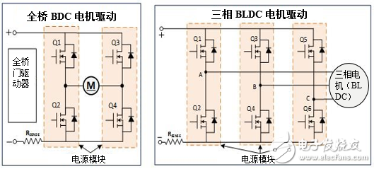
Figure 1: Power Block MOSFETs in Different Motor Drive Topologies
Let's take a look at the advantages that these power blocks can bring to the design of the motor drive subsystem for cordless tools.
Power density multiplicationThe dual-stack chip technology in the CSD885x power block doubles the printed circuit board (PCB) area and reduces PCB footprint by 50% compared to discrete MOSFETs.
Compared to discrete MOSFETs of the same performance class (5mm & TImes; 6mm), the power block that integrates two FETs in the same package reduces the three-phase PCB area used for the inverter topology by 90 mm2 (3 x 5mm-6mm). MOSFET interconnect tracks will operate in PCBs with discrete MOSFETs, and higher operating currents require a wider PCB trace, so PCB size savings are actually well over 90 mm2. Most cordless power tool applications use at least four layers of PCB with a copper thickness greater than 2 ounces. Therefore, saving PCB size through the power module can greatly save PCB cost.
Clean MOSFET switch with low parasiticsFigure 2 shows the parasitic inductance and capacitance caused by component leads and non-optimized layout in a power stage PCB design. These PCB parasitics can cause voltage ringing, which can cause voltage stress on the MOSFET.
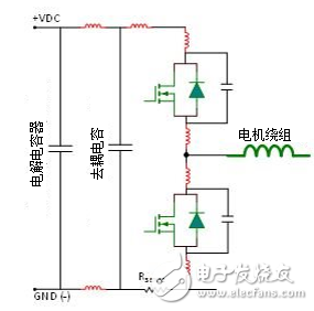
Figure 2: Parasitic inductance and capacitance in a power stage half-bridge.
One of the reasons for ringing is the reverse recovery of the diode. The high current rate of change caused by the fast switching may result in a high diode reverse recovery current. The reverse recovery current flows through the parasitic layout inductance. The resonant network formed by the FET capacitance and parasitic inductance causes the phase node to ring, reducing the voltage margin and increasing the stress on the device. Figure 3 shows the phase node voltage ringing with discrete MOSFETs due to circuit parasitics.
When using a power module, a switch node clamp with two MOSFETs connected keeps the parasitic inductance between the high-side and low-side MOSFETs at an absolute minimum. Using low-side and high-side FETs in the same package minimizes PCB parasitics and reduces phase node voltage ringing. Using these power modules helps ensure a smooth drive MOSFET switch, even when the current is up to 50A, there is no voltage overshoot, as shown in Figure 4.
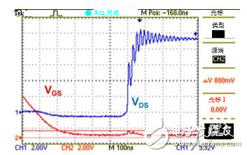
Figure 3: Phase node voltage ringing and voltage overshoot with discrete MOSFETs
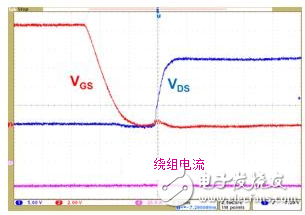
Figure 4: Clean Phase Node Switching Waveform with Power Module
Low PCB loss, reduced PCB parasitic resistanceThe power block helps reduce the length of the high current carrying track in the PCB, thereby reducing power loss in the track.
Let us know the PCB track requirements for discrete FETs. The PCB track connection between the top and bottom partial MOSFETs results in I2R losses in the PCB. Figure 5 shows the copper track when the top and bottom partial MOSFETs are connected side by side; this is one of the common layouts that make it easy to connect the motor windings to the PCB. The length of the copper area connecting the phase nodes is twice the width (the track width depends on the current, and the track width is usually limited by the board's external dimensions). Alternatively, you can arrange the top and bottom discrete MOSFETs up and down between the phase nodes. However, due to the need to provide a motor winding to the phase node, you may not be able to reduce the track length and this arrangement may not be suitable for all applications.
If the designed PCB copper thickness is 2 oz (70 μm), the single-layer PCB track connecting the phase nodes shown in Figure 5 will have a resistance of about 0.24 mΩ. Assuming that the track is present in two PCB planes, the equivalent PCB resistance is 0.12 mΩ. For three-phase power stages, you have three such PCB tracks. You can also perform a similar analysis of the DC power input and return rails.
Power modules have top-side and bottom-side MOSFETs in a single package, and phase nodes connected by metal clips in the package to optimize parasitic resistance and provide flexibility in layout and save a minimum of 0.5 to 1mΩ total PCB resistance .
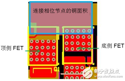
Figure 5: Typical phase node track length with discrete MOSFET
Excellent heat dissipation, double coolingThe CSD885x power module is available in a DualCoolTM package that dissipates heat from the top of the package, dissipating heat from the board, providing excellent thermal performance and increasing power in a 5mm & TImes; 6mm package. According to the data sheet specification, the power block has a junction-to-bottom thermal resistance of 1.1 °C/W and a junction-to-top thermal resistance of 2.1 °C/W. You can optimize the cooling function of the heat sink of the top cover of the PCB or power block of the power block bottom case. Figure 6 shows the results of a top-side common heat sink (27mm × 27mm × 23mm) tested with three CSD88599Q5DC dual-cooled 60V power modules in a 1kW, 36V three-phase inverter PCB (36mm × 50mm). airflow. During testing, the heat sink and power block top case are used with low thermal impedance (Rθ
Shenzhen Linx Technology Co., Ltd. , https://www.linxheadphone.com
