(I) Addition of test points
Test point selection:
Test points are evenly distributed throughout the PBA board.
The device lead-out pins, test pads, connector pins and vias can all serve as test points, but vias are the worst-case test points.
The patch element preferably uses a test pad as a test point.
Each network line should be added with a test point when wiring. The test point should be as far away from the device as possible. The distance between the two test points should not be too close. The center distance should be 2.54mm; if there is already a PAD or Via on a network line, You can not add another test pad.
Do not use the pads of the patch components on the bottom layer as test points.
Leave more than 10 test points for the power supply and ground and distribute them evenly across the entire PBA board to reduce the impact of the reverse drive current on the potential of the entire PBA board during testing, and to ensure that the entire PBA board is equipotential.
When testing PBA boards with batteries, jumpers should be used to prevent short circuits around the battery from being detected.
When adding test points, additional lines should be as short as possible, as shown below:
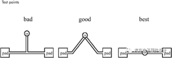
1. Test point size selection.
There are three sizes of test points:
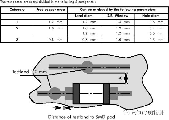
Where: A=1.0mm, B=0.40mm
Note:
Test points can be via pads, surface pads, and vias, but the via must have accessible copper.
When using surface pads as test points, test points should be placed on the solder surface as much as possible.
(II) Labeling of PCB Boards
1. The component and solder surface should have the PCB or PBA number and version number. In the board's welding surface marked the light board number, marked on the component surface mounted welding number, the assembly number is generally behind the light board number plus 1.
2. When labeling, the top layer (first layer) should be a component surface, and it is a positive shape, while the welding surface is an inverse shape.
(Horizontal mirroring), such as the character 'b', is shown as 'b' in the component plane, and the welding surface is shown as 'd'.
3. For screen printing, the silkscreen characters should have a height of 1.5~2.0mm and a line width of 0.2~0.254.
4. PCB layer identification
To identify and name different layers of PCBs for multilayer board production inspections (as in lamination)
1) Edge Layer Marking of Multilayer Boards
The edge layer is identified as: on the edge of the board, a 1.6mm wide and 1.0mm thick copper is placed on the respective layer
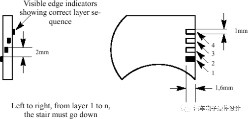
2) Multilayer board layer identification and naming
In order to meet the process requirements of PB production and increase the readability of PB, the layer number should be added on the multilayer board as shown in the figure:
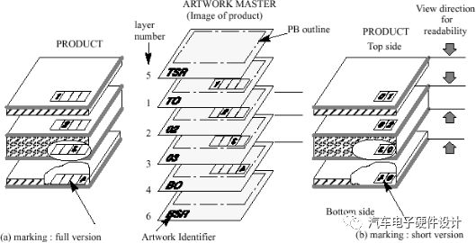
A. Multilayer board numbering principle:
For the top layer and the bottom layer, there are fixed numbers: Top Layer is KK; Bottom Layer is KA. The middle layer number is from bottom to top: KA, KB, KC, KD ... KK
(where KI is not used). The maximum can be expressed as 10 layers, as shown below: (There are two ways to indicate, it is recommended to use the second)
| 1. For 2-layer boards: | ||
| TopLayer | KK | 1 |
| Bottom | KA | 2 |
| 2. For 4-layer boards: | ||
| TopLayer | KK | 1 |
| Middle level 1 | KC | 2 |
| Middle 2 floors | KB | 3 |
| Bottom | KA | 4 |
| 3. For 6-layer boards: | ||
| TopLayer | KK | 1 |
| Middle level 1 | KE | 2 |
| Middle 2 floors | KD | 3 |
| Middle 3 floors | KC | 4 |
| Middle 4 floors | KB | 5 |
| Bottom | KA | 6 |
| 4. For 8-layer boards: | ||
| TopLayer | KK | 1 |
| Middle level 1 | KG | 2 |
| Middle 2 floors | KF | 3 |
| Middle 3 floors | KE | 4 |
| Middle 4 floors | KD | 5 |
| Middle 5 floors | KC | 6 |
| Middle 6 floors | KB | 7 |
| Bottom | KA | 8 |
| 5. For 10-layer board: | ||
| TopLayer | KK | 1 |
| Middle level 1 | KJ | 2 |
| Middle 2 floors | KH | 3 |
| Middle 3 floors | KG | 4 |
| Middle 4 floors | KF | 5 |
| Middle 5 floors | KE | 6 |
| Middle 6 floors | KD | 7 |
| Middle 7 floors | KC | 8 |
| Middle 8 floors | KB | 9 |
| Bottom | KA | 10 |
6. When the board has 12 layers, change the previous letter K to L for 12 layers as follows
As shown, the 12-layer board is analogized.
| TopLayer | KK | 1 |
| Middle level 1 | LB | 2 |
| Middle 2 floors | LA | 3 |
| Middle 3 floors | KJ | 4 |
| Middle 4 floors | KH | 5 |
| Middle 5 floors | KG | 6 |
| Middle 6 floors | KF | 7 |
| Middle 7 floors | KE | 8 |
| Middle 8 floors | KD | 9 |
| 9 layers in the middle | KC | 10 |
| 10 layers in the middle | KB | 11 |
| Bottom | KA | 12 |
B. Multilayer layer numbering principle
The labeling principle is:
The label for each layer should be placed on its own layer, using the text of the current layer (TEXT)
The label of the top layer is a positive character (positive character) from the top layer to the bottom layer; and the bottom layer (Bottom layer) label is an anti-character (anti character) from the top layer to the bottom layer.
The other layers are numbered from the top layer to the bottom layer, odd numbers are anti-characters, and even numbers are positive characters. The following is an example of a 6-layer board. An example is shown below:
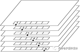
One of the black squares is the edge of the layer logo.
(III) Generation of Processing Data Files and Description of PCBs
1. PCB thickness and copper foil thickness
1) When it is necessary to control the characteristic impedance of the PCB, the thickness of each layer of material may be explained, or
Ask the manufacturer to control the characteristic impedance.
2) The thickness of PCB is 1.0mm, 1.5mm, 1.6mm, 2.4mm, 3.2mm,
4.4mm and so on.
For common PCB thickness is usually 1.6mm
For the backplane thickness is usually 3.2mm (specifically 2.4mm or 4.4mm)
The copper foil thickness of the PCB is 5μm (μm or less μ), 9μ, 12μ, and 17.5μ.
35μ, 70μ, and 105μ.
For a typical PCB, the thickness of the inner copper foil is usually 35μ; the outer layer is 17.5μ, and for special PCBs, 35μ and 70μ (for example, power boards) can be used.
The backplane PCB copper foil thickness is usually 17.5μ or 35μ.
2. Processing data file generation
After the designer completes the design of the PCB, the files required for production and assembly must be generated, which are:
PCB production required documents:
GERBER files (glottes) and DRILL files (drillhole files)
The Gerber file, which contains the D code, is the extended Gerber format file. In addition to the layers
Gerber files also provide positive and negative solder masks, assisted soldering, and screen Gerber data according to the situation, and indicate the content of each document separately.
(NC) Drilling files, to distinguish between holed holes, non-apertured holes (especially assembly holes should be described as non-apertured holes), and the location of shaped holes. And provide CNC drilling tool charts.
To explain is a few layers.
PBA assembly required files:
For VeriBest software it is necessary to output the file in the following format: GENCAD (MITRON CAD FILE)
ODB++
For Mentor software it is necessary to output the file in the following format:
/design/pub:trace (traces.traces_rev#) tech
Layers apeture_table(thermal pads) test points(optional)
four. Glossary
(a) Pore, non-pored, via, shaped, and assembly holes.
Plated through holes: Plated through holes are metallized holes that conduct electricity.
Nu-Plated through holes are not metallized and do not conduct electricity, usually assembly holes.
The vias are holed, but generally do not have devices, usually vias.
Shaped holes are shapes that are not circular, such as oval, square holes.
Mounting holes are holes for mounting the device or fixing the printed board.
(b) Positioning holes and optical positioning points.
Positioning holes are non-porous holes for circuit board production placed on the edge of the board.
Optical positioning points are special pads placed on the board for component placement and board test positioning to meet the automation needs of the board.
(iii) Negative and Positive.
Negative refers to a region that appears to be transparent in computer and film where there are substances (such as copper foil, solder mask, ...). Negative film is mainly used for the inner layer. When there is a large area of ​​copper, using a positive film will produce very large data, resulting in the inability to draw light, so negative film is used.
Positive and negative are the opposite.
(d) Reflow Soldering and Wave Solder.
Reflow Soldering: A welding process that melts the solder that has been placed on a solder joint to form a solder joint. Mainly used for surface mount component welding.
Wave Solder: A process that can weld a large number of solder joints, that is, by soldering the printed solder on the crest of molten solder. Mainly used for the welding of pin elements.
(v) PCB and PBA
PCB (Print Circuit Board) is printed circuit board, also called PB.
PBA (Printed Board Assembly) refers to the assembly of components after the circuit board.
Linear Comparators,Ic Linear Comparators,Ics Linear Comparators,Integrated Circuits Linear Comparators
Shenzhen Kaixuanye Technology Co., Ltd. , https://www.iconlinekxys.com
