Marc Goldfarb, Ben Walker, Russell MarTIn, Tom Bosia, Ed Balboni, and Dragoslav Culum
Analog Devices
Wireless base stations were once packaged in large spaces with climate control technology, but can now be installed anywhere. As wireless network service providers attempt to achieve global signal coverage, base station component providers are under pressure to provide more functionality in smaller packages.
A pair of integrated circuits (ICs) from Analog Devices offers a solution that redefines the meaning of the receiver front-end mixer. In fact, the IC integrates many components that have been added to the in-receiver mixer, such as local oscillator (LO) and intermediate frequency (IF) amplifiers, within the mixer IC. With these ICs, the size of cellular base stations can be drastically reduced, while providing software-defined radio (SDR) flexibility to handle many different wireless standards.
The ICs referred to here are the ADRF6612 and ADRF6614, which are designed to support RF ranges from 700 Mhz to 3000 MHz, LO ranges from 200 Mhz to 2700 MHz, and IF ranges from 40 Mhz to 500 MHz. They support low-side or high-side LO injection, including an on-board phase-locked loop (PLL) and multiple low-noise voltage-controlled oscillators (VCOs), all packaged in a 7 mm &TImes; 7 mm 48-pin LFCSP case. Ultra-high integration and component density, combined with versatility and programmability, can support a wide range of different wireless standards to meet the low-volume production needs of modern microcells.
To better understand the space-saving advantages of these highly integrated mixer ICs, recall the front end of the cellular base station around 2010, as shown in Figure 1. The dual mixer architecture has a bandwidth range of approximately 1 Ghz and requires multiple components to handle the then cellular frequency range, 800 MHz to 1900 MHz. Frequency synthesis is provided by a separate PLL and narrowband VCO module that requires a unique PLL loop filter for optimum performance. A dedicated VCO module is used for each target band, which results in an increase in the board area required in the base station.
In addition, these discrete components are interconnected by low-impedance transmission lines, resulting in increased signal loss. As a result, a large current is required to drive the VCO output to a sufficient level so that the mixer can produce low phase noise and noise figure under signal blocking conditions.
Receiver ICs with integrated VCOs are not new. However, to achieve wide bandwidth and low phase noise for multi-carrier requirements, Global System for Mobile Communications (MC-GSM) wireless networks have always been a challenge. The GSM channel multiplexing scheme requires that the receiving LO have very low phase noise, especially if the phase-to-phase channel offset frequency is 800 kHz, as shown in Figure 2. If the unwanted phase noise of these phase channels is mixed with an unwanted signal that is also at 800 kHz offset, phase noise can be converted to an IF output, reducing system sensitivity.
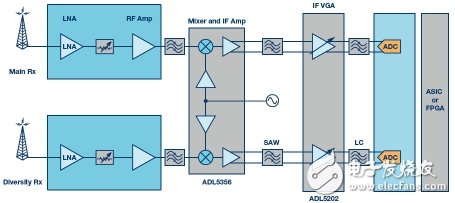
Figure 1. The block diagram shows a typical cellular base station at around 2010.
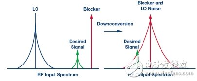
Figure 2. The channel reuse scheme requires the use of a wide-bandwidth VCO with low phase noise in GSM wireless systems to avoid performance degradation due to blocking.
Low VCO phase noise is typically achieved with high quality factor (high Q) resonators and narrowband designs. Frequency division also reduces noise. By operating the VCO at an integer multiple of the receiver LO frequency, the subsequent division can reduce the phase noise by a factor of 6 dB/octave, as shown in Figure 3. GSM's phase noise requirements are extremely high in the 1800 Mhz to 1900 Mhz band, which is approximately twice as high as the phase noise in the 800 Mhz to 900 Mhz band.
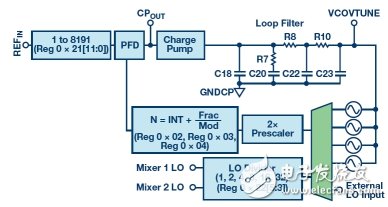
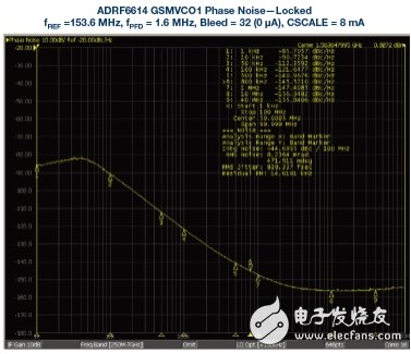
Figure 3. This VCO circuit configuration enables octave bandwidth.
In addition to low phase noise, modern base station receiver designs must support multiple modulation schemes currently used by wireless communication networks. In addition to GSM, other modulation schemes include Wideband Code Division Multiple Access (WCDMA) and Long Term Evolution (LTE) systems. The receiver design typically includes a number of different VCOs whose phase noise performance is configured to a medium level that meets the base station octave bandwidth requirements in a combined manner.
Once several VCOs are configured to produce an octave bandwidth at the highest operating frequency, a lower LO frequency can be achieved with a divide by two. This method is used by the ADRF6612 receiver mixer, where the VCO has a fundamental frequency range of 2.7 Ghz to 5.6 Ghz and achieves an LO frequency of 200 Ghz to 2700 Mhz by dividing the frequency from 1 to 32. For applications that include both MC-GSM, the ADRF6614 receiver mixer includes two additional high-performance VCO cores to provide the LO frequency required for the 1800 Mhz to 1900 MHz GSM band.
Because modern wireless microcells may not have the advantage of a climate controlled environment, components such as these receiver ICs provide consistent, reliable performance over a wide range of extreme temperatures. To achieve the specified performance over a wide operating temperature range, the PLL and VCO in the ADRF6612 and ADRF6614 ICs use a variety of calibration techniques.
For low noise wide bandwidth, each VCO core uses an 8-bit capacitive digital-to-analog converter (CDAC) that selects the correct frequency band for a given LO frequency (128 out of 1). The system carefully monitors any changes in the VCO resonator amplitude and adjusts the amplitude with an automatic level control (ALC) system to achieve the best output amplitude. Each IC performs a calibration sequence when the operating frequency is reprogrammed. This ensures that the selected frequency band concentrates the tuning voltage of the VCO tuned varactor to an optimum range, keeping the frequency synthesizer locked for the desired operating temperature range.
Each of the four VCO cores in the ADRF6612 and ADRF6614 ICs ensures proper overlap of their operating range and can accommodate different environmental conditions and device manufacturing tolerances. For environmental and process differences, the core typically moves in the same direction, thus providing ample overlap mechanism that allows the frequency synthesizer to always implement locking conditions.
Once the calibration scheme is determined, the frequency can be maintained indefinitely, and the tuning voltage range supports the required synchronization range. In a time division duplex (TDD) system, the base station may change the frequency according to different time slots, and its working time may be in microseconds. In a frequency division duplex (FDD) system, it may take many years to lock a single frequency.
Downtime accidents are not allowed at all times during the operation of the ADRF6612 and ADRF6614 IC systems. Therefore, temperature variations and component aging effects are handled by the VCO's varactor tuning voltage range and frequency tuning sensitivity (kV), which may range up to 145 °C. Each IC continuously monitors the device temperature and adjusts the VCO bias as needed.
The ADRF6612 and ADRF6614 Ic use a unique approach to minimize receiver degradation due to spurious signal products. The use of the frequency synthesizer's integer mode and compact loop filter allows reference spurious products to be as low as −100 dBc. The minimum spurious signal is critical to the modulation scheme, such as MC-GSM. For LTE and other modulation schemes, or where a fine frequency step is required, the frequency synthesizer can operate in fractional-N mode. The reference path integrates a 13-bit divider, and the integer and fractional paths each integrate a 16-bit divider for great flexibility.
For applications that require a co-located phase tracking receive channel, such as a Multiple Input Multiple Output (MIMO) system, the ADRF6612 and ADRF6614 ICs can be daisy-chained to allow one of the cells to act as the primary frequency synthesizer, respectively. The external LO output and input ports power other slave receivers. This minimizes the corresponding increase in the extra LO distribution amplifier and its phase noise.
To support both high-end and low-side LO injection, the LO chain of each IC provides flexible signal processing, as shown in Figure 4. Using an integer division ratio of 1 to 32, low-end injection is possible even in the 700 Mhz band and high IF. The LO stage provides a square wave drive for the passive mixer core over the entire LO range from 200 Mhz to 2700 Mhz. 1
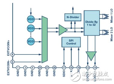
Figure 4. This LO signal chain is used to support a wireless base station receiver.
The in-band signal of a modern wireless base station is close to a low level input signal in frequency, and thus the cellular receiver can act as a blocking signal. In this case, above the target signal, the phase noise from the LO amplifier near the blocking signal is mixed into the IF output band. This will increase the noise floor and sometimes significantly reduce the receiver's signal-to-noise ratio (SNR).
Since the blocking signal can be large (high power), the VCO phase noise must be extremely low and the LO chain does not reduce the noise floor under the occlusion device offset condition. At these very high blocking levels, the receiver noise figure is eventually dominated by the blocking signal and falls according to the level of the blocker power level.
In a discrete receive chain approach, some filtering mechanisms can be introduced on the LO path to minimize phase noise from the VCO and LO distribution amplifiers under occluder offset conditions. However, in an integrated front end, care must be taken to avoid additive phase noise in the LO chain.
The ADRF6612 and ADRF6614 ICs use a high gain LO chain and a hard limiting amplifier to drive the LO chain to the limit. When each stage enters a hard limit, the gain of the LO chain small signal, which in other cases increases the phase noise, will be greatly reduced, thereby minimizing the noise figure reduction under blocking conditions.
Noise folding from the blocking signal reduces the receiver output noise spectral performance and increases the output noise floor, thereby reducing the receiver noise figure. The ADRF6612 and ADRF6614 receiver ICs are designed to withstand large blocking signals while minimizing receiver noise figure degradation, as shown in Figure 5. Even with an input blocking level of 10 dBm, the receiver's noise figure will only drop by 3.2 dB at a carrier offset of 10 MHz, even if the conversion gain is reduced by 1 dB at the extreme blocking level.
These receiver ICs have an extremely high level of integration, which can greatly improve performance and save DC power consumption for modern wireless base station designers, as shown in Figure 6. The IC uses a technology that optimizes both RF and IF levels around the on-chip mixer. 2
This technology is the first to be used in the ADRF6612 with a minimum IIP3 of over 25 dBm over the entire temperature range and over the entire frequency range and low power consumption, and 29 dBm to 2 GHz over temperature. The technique also has the best receive path noise figure performance and high conversion gain, as shown in Figure 7. 3,4
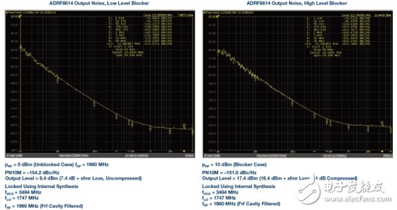
Figure 5. This figure compares the output noise spectrum of the ADRF6614 receiver IC with low and high blocking signals (left and right, respectively).
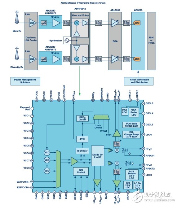
Figure 6. This signal chain shows the components used in a typical wireless base station receiver.
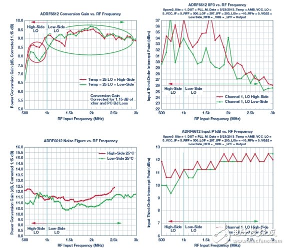
Figure 7. The measured gain, noise figure, and input third-order intercept point (IIP3) of the ADRF6612 receiver IC are shown.
AcknowledgementAs the integration within the complete receiver chain increases, so does the size of the development team. Although it is not possible to list all the people who contributed to this article, the authors are honored to express their sincere gratitude to the following industry experts: Kurt Fletcher and Dominic Mai spent a lot of time to achieve excellent layout and maintain symmetry, avoiding useless coupling . Vincent Bu works closely with our suppliers to develop the necessary packaging. Susan Stevens maintains a good working relationship with external foundry partners. Craig Levy and Rachana Kaza developed production test capabilities for these devices. Wendy DuTIle, Ed Gorzynski and Chris Norcross are all involved in the extensive prototyping of test circuits. Mark Hyslip is responsible for business coordination and has shaped the project. The author of this article hopes to commemorate our colleague, Edward J. Gorzynski.
- [Worldwide Compatibility]With a worldwide 100-240V AC input, it's a truly global charger and perfect for international traveling. Compatible with iOS, Android, & Windows smart phones as well as tablets, speakers, cameras, and other 5V USB devices
-
With 9 years experience in the filed, Shenzhen WAWEIS Technology Co., Ltd is one of the best power supply device manufacturer in China. Our world-class production plant passed ISO9001:2008 & ISO14001:2004 certifications and is equipped with the state-of-art technology and machines. The main products we make are power adapters, which can be used in laptop, LCD display, LED lights, CCTV camera(12v series), Speaker(24v series), Balance car(42v series). All our products comply with European environmental standard as well as CCC,RoHS ,CE , FCC.
Ungrouped,High Quality Ungrouped,Ungrouped Details, CN
Shenzhen Waweis Technology Co., Ltd. , https://www.laptopsasdapter.com
