
In the field of mobile communications, omnidirectional high gain antennas have a wide range of applications. As an omnidirectional high-gain antenna, the microstrip cross-over antenna is characterized by its simple structure, easy matching, convenient mass production and low cost. The general microstrip cross-element antenna is shown in Figure 1. In this simulation and actual measurement, the distortion of the pattern is more serious, and the voltage standing wave ratio of the antenna is also poor. The literature gives an improved solution to make the ground of the microstrip antenna into a trapezoidal structure, as shown in Figure 2. This improves the antenna performance to some extent. The simulation and physical test results of the structure antenna are given in order to compare with the microstrip omnidirectional antenna proposed in this paper. The microstrip omnidirectional antenna proposed in this paper is shown in Figure 3. In addition to the microstrip gradation structure and the inductive matcher, the antenna is also loaded with a λg/4 short-circuit matching branch at the top of the antenna. Simulation and testing show that the antenna has a better voltage standing wave ratio and higher gain than the antenna proposed in the literature. It is a high performance microstrip omnidirectional antenna.
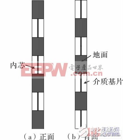
Figure 1 Schematic diagram of a microstrip cross-element antenna
1 Basic principle of microstrip crossover antennaThe basic structure of the microstrip cross-over antenna is shown in Figure 1. The ground of each microstrip transmission line is regarded as the outer conductor of the coaxial line, and the conduction band is regarded as the inner conductor of the coaxial line, which has a similar structure to the conventional COCO antenna. Similarly, the microstrip cross-element antenna is also formed by cascading a plurality of λg/2 microstrip units, and the ground and conduction bands of the antenna are alternately placed on both sides of the dielectric substrate, thereby implementing the phase inversion by using the cross connection. Since the discontinuity of the cross-connection points forms radiation, there are two modes of this structure, namely, a transmission mode and a radiation mode. For the transmission mode, since the wave is transmitted along the inner surface of the conduction band and the ground plate, and the microstrip transmission line is uniform, the radiation of the space is not considered in the analysis. The radiation mode is because the radiation current excited by the voltage source alternated between the ground plates exists on the inner and outer surfaces of the ground plate to form radiation. Like the COCO antenna, the microstrip cross-element antenna is also an array antenna. According to the basic theory of the array antenna, for the far field region, the normalized directivity function of the antenna is

The gain of the antenna is
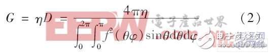
Where η is the radiation efficiency of the antenna; D is the directivity coefficient of the antenna.
2 Design and analysis of microstrip crossover antenna
The basic microstrip cross-element antenna is shown in Fig. 1. The experiment proves that the distortion of the antenna pattern of the structure antenna is serious, and the voltage standing wave ratio in the band is not ideal. In order to improve the performance of the antenna, the antenna floor is designed as a trapezoidal structure, and a rectangular patch is loaded in the middle of each microstrip unit conduction band for tuning the antenna. The antenna structure at this time is as shown in FIG. 2, which is The impedance characteristics of the antenna are improved to some extent. The loaded rectangular patch is equivalent to one inductor. Assuming that the length of the inductor is l and the width is w, the inductance L of its equivalent circuit is as shown in equation (3).
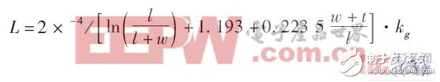
Where h is the thickness of the dielectric plate; t is the thickness of the conductor; Kg is the correction factor, and the empirical formula is
![]()
It can be seen from equation (3) that in the case where the parameters of the dielectric plate are determined, the inductance value of the rectangular patch is mainly determined by its width w.
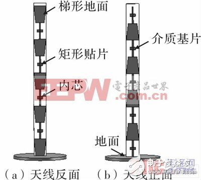
Figure 2 Top unloaded antenna schematic
Microstrip cross-element antennas have similar structures and the same working principles as COCO antennas, so they have similar equivalent circuits. Figure 2 shows the microstrip antenna. The equivalent circuit of each microstrip unit is shown in Figure 4, where R is the equivalent radiation resistance; C is the equivalent capacitance; L is the equivalent inductance. L includes the inductance of the microstrip unit itself and the loaded inductance. They form an RLC resonant circuit. Before the antenna is loaded with the rectangular patch, its characteristic impedance exhibits a large capacitive reactance. Therefore, by adjusting the width of the rectangular patch, the size of the loaded inductor is changed to obtain the best S11.
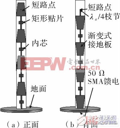
Figure 3 Schematic diagram of a microstrip cross-element antenna with a top-loaded short-circuit matching branch
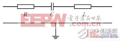
Figure 4 The equivalent circuit of the antenna when the top end is not loaded with the short-circuit branch
Figure 5 shows the S11 of the antenna at different values. Optimized, when w=6, the antenna at this time has the best matching performance. At this time, the antenna S11 is -15 dB in the band.
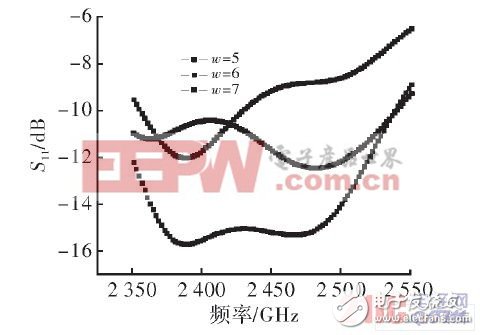
Figure 5 Antenna S11 with different W values ​​when the top is not loaded
In order to further reduce the energy reflection of the antenna and improve the radiation characteristics of the antenna, a λg/4 short-circuit matching branch is loaded at the top of the antenna, and the antenna structure is as shown in FIG. After loading at the top of the antenna, the equivalent circuit of each microstrip unit is shown in Figure 6, which is equivalent to an admittance connected in parallel on the microstrip unit. Wherein, R1 is the equivalent radiation resistance of the microstrip unit; C1 is an equivalent capacitance; L1 is an equivalent inductance; Y is an equivalent admittance of the top shorting branch.
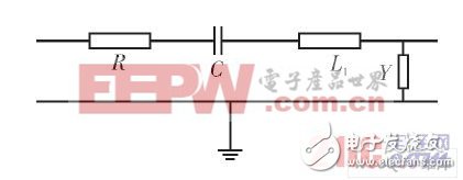
Figure 6 The equivalent circuit of the antenna after the top loading
The admittance Y of the short-circuit matching branch adjusts the impedance matching of the entire antenna. According to the Smith chart, when the top of the antenna is not loaded with the λg/4 short-circuit matching branch, at 2 400 to 2 483.5 MHz, the real part of the antenna impedance is between 37 and 46 Ω. After loading the matching branch, the characteristic impedance of the antenna The real part is between 47 and 58 Ω. Moreover, the imaginary part of the antenna impedance also has a significant change, and its value is closer to zero in the required frequency band. Figure 7 and Figure 8 show the real-time and imaginary parts of the impedance obtained by the CST simulation software for the two antennas as a function of frequency. It can be seen from the figure that after the λg/4 short-circuit matching branch is applied to the top of the antenna, the real part of the antenna impedance increases significantly, and the imaginary part also decreases compared to when it is not loaded. Figure 9 shows the effect of different w on antenna S11 after the top loading shorts match the branch. As can be seen from the figure, when w is 6, the antenna is S11-20 dB in the required frequency band.
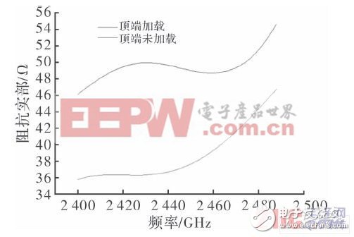
Figure 7 Antenna impedance real part with frequency curve
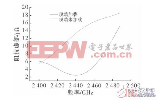
Figure 8 Antenna impedance imaginary part with frequency curve
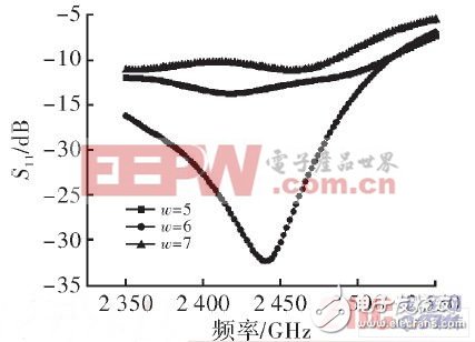
Figure 9 Antenna S11 with different W values ​​after the top is not loaded
After the top of the antenna is loaded with the λg/4 short-circuit matching branch, the current distribution on the antenna changes accordingly. When the wave passes to the top of the antenna and passes through the λg/4 unit, it produces a 90° phase shift. When the short-circuit point passes, a 180° phase shift occurs, and when it passes through the λg/4 ground, a 90° phase shift is generated. After the current is shorted to match the branch, a phase shift of 360° is produced. The current after phase shifting has the same phase as the original excitation current, thereby acting as a current compensation for the antenna and maintaining the balance of the current on the antenna.
The physical object of the antenna is shown in Figure 10. The antenna uses a dielectric plate with a thickness of 1.5 mm and a relative dielectric constant of 2.65, and the bottom is fed with a 50 Ω SMA connector. In actual production, the antenna array length is slightly smaller than the simulation length, which is caused by the loss of material. In general, the bottom side of the antenna trapezoidal ground is λg/2, and the length of the rectangular patch is slightly smaller than the short side of the trapezoidal ground. The length of the λg/4 matching branch at the top is also slightly less than 1/4 of the operating wavelength of the antenna.
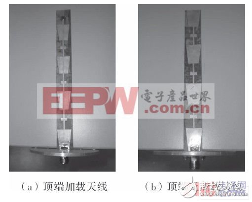
Figure 10 Antenna of the object
Table 1 and Figure 11 show the comparison of the measured gains of the two antennas and S11, respectively. It can be seen that the antenna gain is increased by 1 to 1.3 dBi after the antenna tip is short-circuited. This is because the top loading short-circuit matching branch improves the impedance matching performance of the antenna, improves the radiation efficiency of the antenna, and reduces the reflection of energy on the antenna, so that the radiation power obtained on each microstrip unit is maximized. The aperture efficiency of the antenna is utilized, thereby increasing the gain of the antenna.
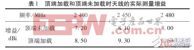
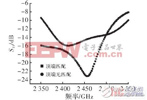
Figure 11 Actual measurement of top loading and top unloaded antenna
3 ConclusionThe CST simulation results of the two antennas are basically consistent with the measured results. Comparing the actual test results with the simulation results, it is found that the measured gain of the antenna is slightly higher than that obtained by the simulation software, which is mainly due to the influence of the earth on the antenna. After loading the λg/4 short-circuit matching branch at the top of the antenna, the VSWR of the antenna is further reduced, and the gain is improved. The antenna is physically cascaded with 7 microstrip units with a total height of 25 cm. The measured average gain is 9 dBi. If you want to obtain higher gain, you can use more microstrip units for cascading. It is a cost-effective microstrip high-gain omnidirectional antenna.
LED Par can
LED PAR LIGHT Series
54X3W rgbw; 18x12w RGBW;24x12w RGBW is hot selling in the market. It have waterproof and non-waterproof
Features:
- RGBWA+UV color, 6-in-1 LEDs, excellent color mixing
- quiet working, suitable for quiet applications like theater, studio,etc
-
suitable for events where indoor/outdoor flexibility is needed
- Adjustable PWM (Pulse Width Modulation) to avoid flickering on camera
- Advanced optics provide exceptional color mixing and high efficiency
- Smooth dimming curves for eliminate flicker and choppiness in fades
Our company have 13 years experience of LED Display and Stage Lights , our company mainly produce Indoor Rental LED Display, Outdoor Rental LED Display, Transparent LED Display,Indoor Fixed Indoor LED Display, Outdoor Fixed LED Display, Poster LED Display , Dance LED Display ... In additional, we also produce stage lights, such as beam lights Series, moving head lights Series, LED Par Light Series and son on...
LED Par Light Series,Led Par Can Lights,Par Can,Led Par Stage Light
Guangzhou Chengwen Photoelectric Technology co.,ltd , https://www.cwstagelight.com