
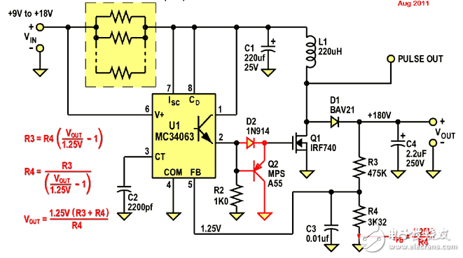
The MC34063 is a monolithic bipolar linear integrated circuit dedicated to the DC-DC converter control section. The chip contains a temperature-compensated bandgap reference, a duty cycle control oscillator, a driver, and a high-current output switch that can output a 1.5A switching current. It can form a switching boost converter, a buck converter and a power inverter with a minimum of external components.
Features:Can work at 3.0-40V input voltage
Short circuit current limit
Low quiescent current
Output switch current up to 1.5A (no external triode)
Adjustable output voltage
Operating oscillation frequency from 100HZ to 100KHZ
MC34063 circuit principle:The oscillator continuously charges and discharges the timing capacitor externally connected to the CT pin (pin 3) through the constant current source to generate an oscillating waveform. Both the charging and discharging currents are constant, and the oscillation frequency depends only on the capacity of the external timing capacitor. The C input of the AND gate is high when the oscillator is externally charged, and the D input is high when the input level of the comparator is below the threshold level. When the C and D inputs are both high, the flip-flop is set high and the output switch is turned on. Otherwise, when the oscillator is discharging, the C input is low and the flip-flop is reset, causing the output The switch is in the off state. The current limit is accomplished by detecting the voltage drop across the resistor between VCC and pin 5. When it is detected that the voltage drop across the resistor is close to more than 300mV, the current limiting circuit starts to work. At this time, the timing capacitor is quickly charged by the CT pin (pin 3) to reduce the charging time and the on-time of the output switch. The off time of the output switch tube is extended.
MC34063 pin diagram and block diagram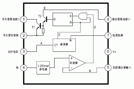
1 pin: the collector terminal of the switch tube T1;
2 feet: the emitter end of the switch tube T1;
3 feet: timing capacitor ct terminal; adjust ct to change the operating frequency within the range of 100-100 kHz;
4 feet: power ground;
5 feet: the inverting input terminal of the voltage comparator, and also the sampling terminal of the output voltage; when using, two precision resistors with an accuracy of not less than 1% should be connected externally;
6 feet: power supply;
7 feet: load peak current (Ipk) sampling end; when the voltage between 6, 7 feet exceeds 300mV, the chip will start the internal overcurrent protection function;
Pin 8: Drive tube T2 collector terminal.
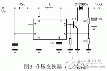
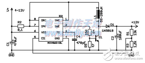
Mc34063 boost circuit diagram (1)The principle of the booster circuit composed of MC34063 booster circuit MC34063 is as shown in the figure below. When the on-chip switch (T1) is turned on, the power supply is grounded through the sampling resistor Rsc, the inductors L1 and MC34063, and the inductor L1 starts to store. Energy, while C0 supplies energy to the load. When T1 is turned off, the power supply and the inductor simultaneously supply energy to the load and the capacitor Co. During the release of energy, the inductance of the electromotive force at both ends is the same as the polarity of the power supply, which is equivalent to the two power supplies connected in series, so that the voltage obtained on the load is higher than the power supply voltage. The frequency at which the switch is turned on and off is called the operating frequency of the chip. As long as the frequency constant of this frequency relative to the load is high enough, a continuous DC voltage can be obtained on the load.
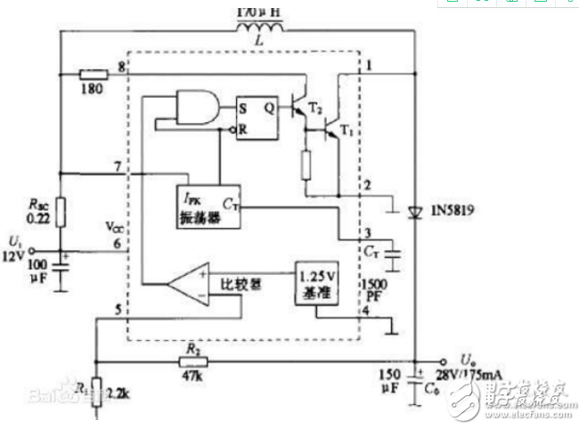
MC34063 boost circuit
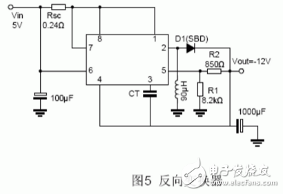
Mc34063 boost circuit diagram (2)MC34063 boost circuit: from 5V to 12V
MC34063 high current buck converter circuit
MC34063 high current boost converter circuit
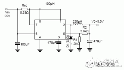
MC34063 Buck Converter Circuit
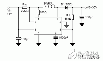
MC34063 boost converter circuit
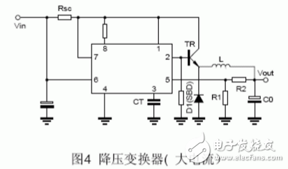
MC34063 boost current-expanding circuit diagram, according to the output voltage, select the appropriate current-expanding transistor, the triode should be added with heat sink, the minimum voltage of this circuit is 4V, the output voltage is 12V, the value of R1 and R3 can be adjusted to change the output voltage.
Circuit Determination The boost type HB LED driver circuit composed of MC34063 is shown in the figure below.
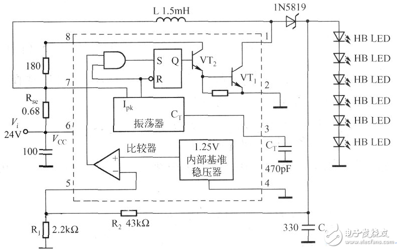
This is a HB LED driver circuit composed of MC34063 with 12V power supply. After boosting, it drives 6 HBLEDs with an output current of 200mA and an operating voltage of about 22V. The duty cycle using the current continuous mode of operation is approximately 0.5.
Wuxi Doton Power , http://www.dotonpower.com